Electromagnetic shielding film, circuit board, and preparation method of electromagnetic shielding film

An electromagnetic shielding film, printed circuit board technology, applied in the field of electronics, can solve the problems of grounding failure, inability to interfere with charge export, inability to achieve shielding function, etc., to achieve the effect of shielding function

Pending Publication Date: 2020-02-07
GUANGZHOU FANGBANG ELECTRONICS
View PDF9 Cites 0 Cited by
  • Summary
  • Abstract
  • Description
  • Claims
  • Application Information

AI Technical Summary

Problems solved by technology

However, at high temperature, the conductive adhesive layer expands and pulls away the conductive particles that were originally in contact with each other or the conductive particles that were originally in contact with the circuit board ground layer, resulting in grounding failure, unable to quickly export interference charges, and unable to realize the shielding function.

Method used


Image

  • Electromagnetic shielding film, circuit board, and preparation method of electromagnetic shielding film
  • Electromagnetic shielding film, circuit board, and preparation method of electromagnetic shielding film
  • Electromagnetic shielding film, circuit board, and preparation method of electromagnetic shielding film

Examples


Embodiment 1

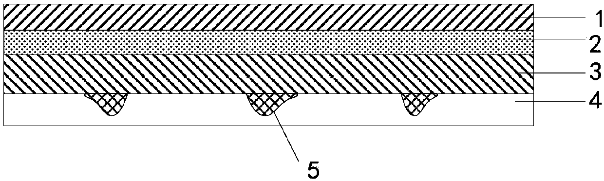
[0072] See figure 1 , the embodiment of the present invention provides an electromagnetic shielding film, which includes a first shielding layer 1, an adhesive layer 2, a second shielding layer 3 and an adhesive film layer 4 stacked in sequence; the second shielding layer 3 is close to the Conductive protrusions 5 are provided on one side of the adhesive film layer 4 . Wherein, the material of the conductive protrusion 5 may be pure metal, alloy or conductive glue with good electrical conductivity, which is not specifically limited here.

[0073] In this embodiment, by providing a conductive protrusion 5 on the side of the second shielding layer 3 close to the adhesive film layer 4, the conductive protrusion 5 ensures that the second shielding layer 5 is The shielding layer 3 can smoothly pierce through the adhesive film layer 4 and contact the ground layer of the circuit board 8, and then ensure that the interference charges are normally exported under the cooperation of the...

Embodiment 2

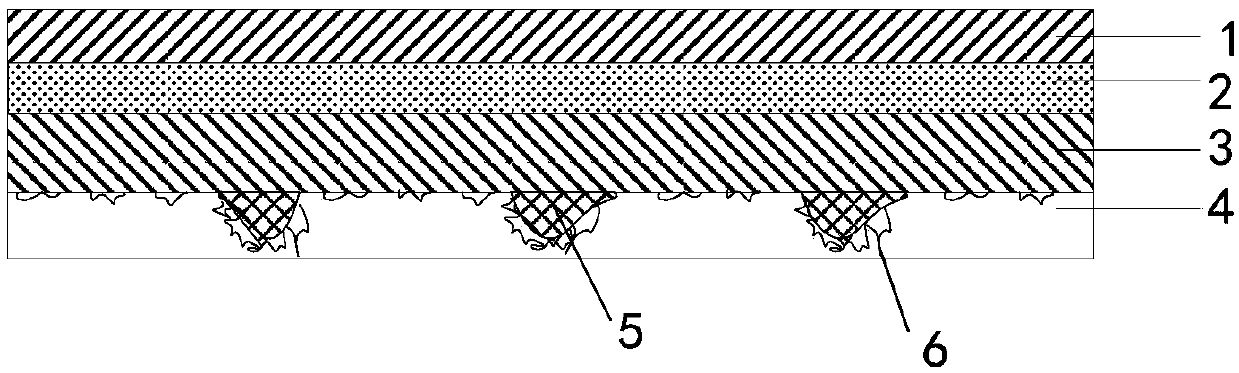
[0103] see Figure 4 , the embodiment of the present invention provides another electromagnetic shielding film, which includes a first shielding layer 1, an adhesive layer 2, a second shielding layer 3, a third shielding layer 7 and an adhesive film layer 4; the first shielding layer 1. The adhesive layer 2 and the second shielding layer 3 are stacked in sequence; the second shielding layer 3 is provided with conductive protrusions 5 on the side away from the adhesive layer 2; the third The shielding layer 7 is covered on the one side of the second shielding layer 3, and the position of the third shielding layer 7 covering the conductive protrusion 5 forms a raised portion 70 (the raised portion 70 is in contact with The relationship between the conductive bumps 5 can be one-to-one correspondence, one-to-many correspondence, or many-to-one correspondence, etc. When the relationship between the raised portion 70 and the conductive bumps 5 is a one-to-one correspondence, the rai...

Embodiment 3

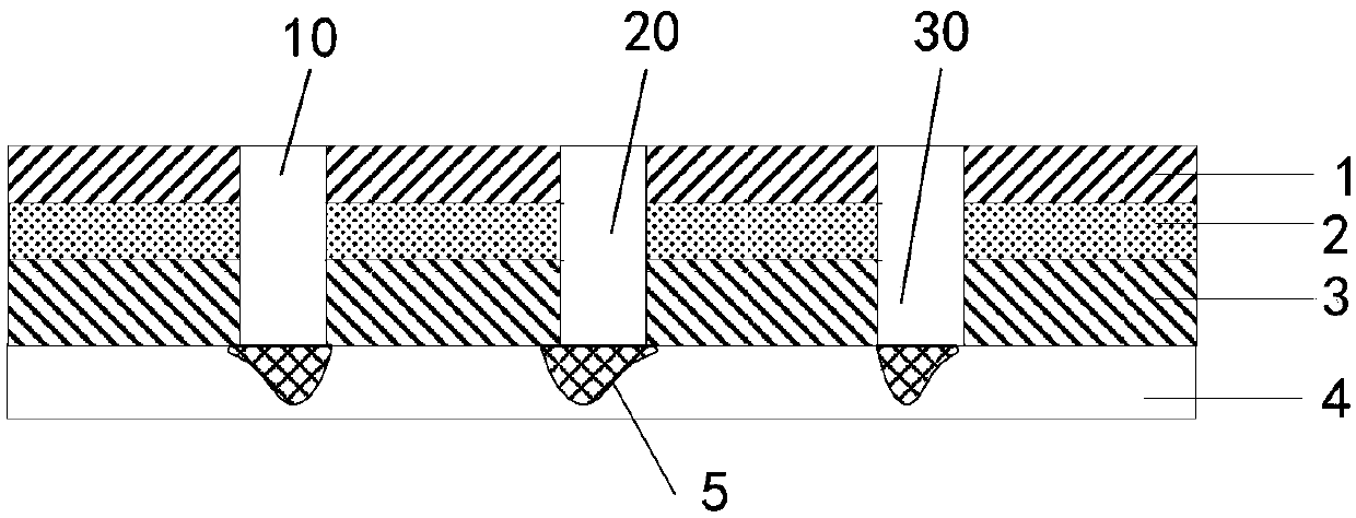
[0116] see Figure 9 and Figure 10 , the embodiment of the present invention provides a circuit board, including a printed circuit board 8 .

[0117] see Figure 9 , the circuit board also includes the electromagnetic shielding film of any solution in the first embodiment; the electromagnetic shielding film is pressed on the printed circuit board 8, and the adhesive film layer 4 is close to the printed circuit board , specifically, the second shielding layer 3 may be in direct contact with the printed circuit board or there is an interval between the two; the conductive protrusion 5 pierces the adhesive film layer 4 and extends to the printed circuit board 8 strata.

[0118] or, see Figure 10, the circuit board also includes the electromagnetic shielding film of any solution in the second embodiment; the electromagnetic shielding film is pressed on the printed circuit board 8, and the adhesive film layer 4 is close to the printed circuit board , specifically, the adhesi...


PUM

PropertyMeasurementUnit
diameteraaaaaaaaaa
melting pointaaaaaaaaaa
thicknessaaaaaaaaaa

Abstract

The invention discloses an electromagnetic shielding film, a circuit board and a preparation method of the electromagnetic shielding film. The electromagnetic shielding film comprises a first shielding layer, a bonding layer, a second shielding layer and an adhesive film layer which are sequentially stacked; and a conductive bulge is arranged on one surface, close to the adhesive film layer, of the second shielding layer. The bulge extends into the adhesive film layer, so that the bulge ensures that the second shielding layer can smoothly pierce through the adhesive film layer when in pressing, the bulge is in contact with a ground layer of the circuit board, and then normal derivation of interference charges is ensured under the cooperation of the first shielding layer, the bonding layerand the second shielding layer, and the shielding function is realized.

Description

technical field [0001] The invention relates to the field of electronics, in particular to an electromagnetic shielding film, a circuit board and a preparation method of the electromagnetic shielding film. Background technique [0002] With the rapid development of the electronics industry, electronic products are further developed toward miniaturization, light weight, and high-density assembly, which greatly promotes the development of flexible circuit boards, thereby realizing the integration of component devices and wire connections. Flexible circuit boards can be widely used in industries such as mobile phones, liquid crystal displays, communications and aerospace. [0003] Driven by the international market, functional flexible circuit boards dominate the flexible circuit board market, and an important indicator for evaluating the performance of functional flexible circuit boards is electromagnetic shielding (Electromagnetic Interference Shielding, referred to as EMI Sh...

Claims


Application Information

Patent Timeline
Patent Type & Authority Applications(China)
IPC IPC(8): H05K9/00H05K1/02C09J7/29C09J9/02B32B3/30B32B7/12B32B33/00
CPCH05K9/0088H05K1/0218C09J7/29C09J9/02B32B3/30B32B7/12B32B33/00H05K2201/0715B32B2307/212B32B2307/202B32B2457/08C09J2301/16C09J2301/122C09J2301/314
Inventor 苏陟
Owner GUANGZHOU FANGBANG ELECTRONICS
Why Eureka
Try Eureka