Electromagnetic shielding film, circuit board and preparation method of electromagnetic shielding film

A technology of electromagnetic shielding film and printed circuit board, which is applied in the field of electronics, can solve the problems of not being able to interfere with the export of charges, unable to realize the shielding function, grounding failure, etc., and achieve the effects of shielding, smooth export, and high shielding

Pending Publication Date: 2020-02-07
GUANGZHOU FANGBANG ELECTRONICS
View PDF21 Cites 0 Cited by
  • Summary
  • Abstract
  • Description
  • Claims
  • Application Information

AI Technical Summary

Problems solved by technology

However, at high temperature, due to the expansion of the conductive adhesive layer, the conductive particles in the conductive adhesive layer that were originally in contact with each other or the conductive particles that were originally in contact with the circuit board ground layer were pulled apart, resulting in grounding failure, and the interference charge could not be quickly exported. , the shielding function cannot be realized

Method used


Image

  • Electromagnetic shielding film, circuit board and preparation method of electromagnetic shielding film
  • Electromagnetic shielding film, circuit board and preparation method of electromagnetic shielding film
  • Electromagnetic shielding film, circuit board and preparation method of electromagnetic shielding film

Examples


Embodiment Construction

[0035] The following will clearly and completely describe the technical solutions in the embodiments of the present invention with reference to the accompanying drawings in the embodiments of the present invention. Obviously, the described embodiments are only some, not all, embodiments of the present invention. Based on the embodiments of the present invention, all other embodiments obtained by persons of ordinary skill in the art without creative efforts fall within the protection scope of the present invention.

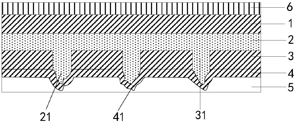
[0036] see figure 1 , is a structural schematic diagram of an angle of the electromagnetic shielding film provided in Embodiment 1 of the present invention;

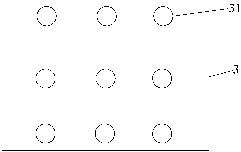
[0037] see figure 2 , is a structural schematic diagram of another angle of the electromagnetic shielding film provided by Embodiment 1 of the present invention;

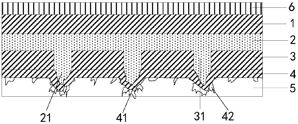
[0038] combine figure 1 and figure 2As shown, the electromagnetic shielding film includes a first shielding layer 1, a conductive adhesive l...


PUM

PropertyMeasurementUnit
heightaaaaaaaaaa
thicknessaaaaaaaaaa
thicknessaaaaaaaaaa

Abstract

The embodiment of the invention provides an electromagnetic shielding film, a circuit board and a preparation method of the electromagnetic shielding film, wherein the electromagnetic shielding film comprises a first shielding layer, a conducting resin layer, a second shielding layer, a third shielding layer and an adhesive film layer, which are sequentially stacked, a first through hole is formedin the second shielding layer, and a protrusion is arranged at the first through hole; the protrusion is formed by the conducting resin layer that flows from one side of the first through hole to theother side at a melting temperature and is immediately cooled; the third shielding layer is arranged on one side of the second shielding layer close to the protrusion and covers the protrusion, and aprotrusion portion is formed on the outer surface of the third shielding layer corresponding to the protrusion, the protrusion portion extends into the adhesive film layer, so that during the press fitting of the protrusion portion, the third shielding layer smoothly pierces the adhesive film layer and contacts a ground layer of the circuit board, and then the normal export of interference charges is ensured under the cooperation of the first shielding layer, the conducting resin layer, the second shielding layer and the third shielding layer, and a shielding function is realized.

Description

technical field [0001] The invention relates to the field of electronics, in particular to an electromagnetic shielding film, a circuit board and a preparation method of the electromagnetic shielding film. Background technique [0002] With the rapid development of the electronics industry, electronic products are further developed toward miniaturization, light weight, and high-density assembly, which greatly promotes the development of flexible circuit boards, thereby realizing the integration of component devices and wire connections. Flexible circuit boards can be widely used in industries such as mobile phones, liquid crystal displays, communications and aerospace. [0003] Driven by the international market, functional flexible circuit boards dominate the flexible circuit board market, and an important indicator for evaluating the performance of functional flexible circuit boards is electromagnetic shielding (Electromagnetic Interference Shielding, referred to as EMI Sh...

Claims


Application Information

Patent Timeline
Patent Type & Authority Applications(China)
IPC IPC(8): H05K9/00
CPCH05K9/0088
Inventor 苏陟
Owner GUANGZHOU FANGBANG ELECTRONICS
Why Eureka
Try Eureka