Electromagnetic shielding film, circuit board and preparation method of electromagnetic shielding film

An electromagnetic shielding film and printed circuit board technology, applied in the field of electronics, can solve the problems of increasing the insertion loss of the circuit board and affecting the integrity of signal transmission, and achieve the effects of reducing the insertion loss, reliable grounding, and strong practicability

Active Publication Date: 2020-07-28
GUANGZHOU FANGBANG ELECTRONICS +1
View PDF3 Cites 0 Cited by
  • Summary
  • Abstract
  • Description
  • Claims
  • Application Information

AI Technical Summary

Problems solved by technology

However, during high-frequency transmission, the conductive particles in the conductive adhesive layer will generate eddy current loss, which will increase the insertion loss of the circuit board and affect the integrity of signal transmission.

Method used


Image

  • Electromagnetic shielding film, circuit board and preparation method of electromagnetic shielding film
  • Electromagnetic shielding film, circuit board and preparation method of electromagnetic shielding film
  • Electromagnetic shielding film, circuit board and preparation method of electromagnetic shielding film

Examples


Embodiment Construction

[0038] The following will clearly and completely describe the technical solutions in the embodiments of the present invention with reference to the accompanying drawings in the embodiments of the present invention. Obviously, the described embodiments are only some, not all, embodiments of the present invention. Based on the embodiments of the present invention, all other embodiments obtained by persons of ordinary skill in the art without creative efforts fall within the protection scope of the present invention.

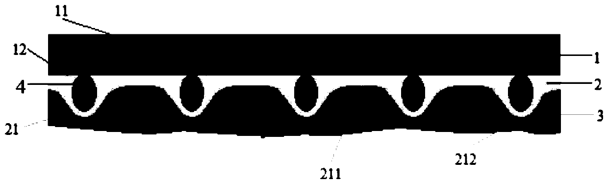
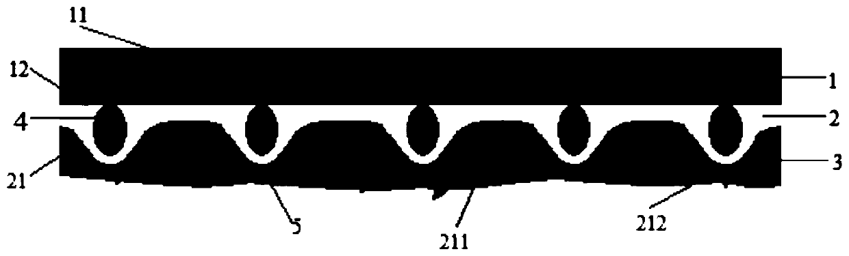
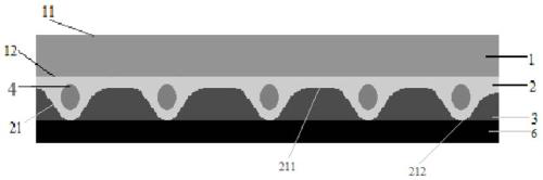
[0039] see figure 1 , is a schematic structural diagram of an electromagnetic shielding film in Embodiment 1 of the present invention, as figure 1 As shown, the electromagnetic shielding film includes a first shielding layer 1, a second shielding layer 2, an adhesive film layer 3 and several convex particles, and the first shielding layer 1 includes opposite first surfaces 11 and second surfaces 12 , the second surface 12 is a flat surface, and the plurality of co...


PUM

PropertyMeasurementUnit
heightaaaaaaaaaa

Abstract

An embodiment of the present invention provides a method for preparing an electromagnetic shielding film, a circuit board, and an electromagnetic shielding film, wherein the electromagnetic shielding film includes a first shielding layer, a second shielding layer, an adhesive film layer, and several convex particles; The first shielding layer includes opposite first surfaces and second surfaces, and the second surface is a flat surface; the plurality of convex particles are attached to the second surface of the first shielding layer; the second shielding layer a layer is disposed on the second surface of the first shielding layer and covers the plurality of convex particles, thereby forming protrusions on the outer surface of the second shielding layer at positions corresponding to the convex particles, In other positions, a gentle portion is formed; the adhesive film layer is arranged on the outer surface of the second shielding layer, and the raised portion ensures that the shielding layer penetrates the adhesive film layer smoothly during the pressing process, ensuring that the interference charge It is normally exported, and at the same time, the gentle part of the second shielding layer can reduce the insertion loss during use, which is suitable for UHF transmission.

Description

technical field [0001] The invention relates to the field of electronics, in particular to an electromagnetic shielding film, a circuit board and a preparation method of the electromagnetic shielding film. Background technique [0002] With the rapid development of the electronics industry, electronic products are further developed toward miniaturization, light weight, and high-density assembly, which greatly promotes the development of flexible circuit boards, thereby realizing the integration of component devices and wire connections. Flexible circuit boards can be widely used in industries such as mobile phones, liquid crystal displays, communications and aerospace. [0003] Driven by the international market, functional flexible circuit boards dominate the flexible circuit board market, and an important indicator for evaluating the performance of functional flexible circuit boards is electromagnetic shielding (Electromagnetic Interference Shielding, referred to as EMI Sh...

Claims


Application Information

Patent Timeline
Patent Type & Authority Patents(China)
IPC IPC(8): H05K9/00B32B33/00B32B3/08
CPCB32B3/085B32B33/00B32B2307/212B32B2457/08H05K9/0088B32B3/30B32B5/18B32B5/32B32B7/06B32B7/12B32B2307/748H05K1/0216H05K9/0075H05K9/0083H05K9/0084
Inventor 苏陟
Owner GUANGZHOU FANGBANG ELECTRONICS
Why Eureka
Try Eureka