Electromagnetic interference shielding film, circuit board and preparation method of electromagnetic interference shielding film

An electromagnetic shielding film, printed circuit board technology, applied in the field of electronics, can solve the problems of grounding failure, inability to interfere with charge export, inability to achieve shielding function, etc., to achieve the effect of shielding function

Pending Publication Date: 2020-02-07
GUANGZHOU FANGBANG ELECTRONICS
View PDF8 Cites 0 Cited by
  • Summary
  • Abstract
  • Description
  • Claims
  • Application Information

AI Technical Summary

Problems solved by technology

However, at high temperature, the conductive adhesive layer expands and pulls away the conductive particles that were originally in contact with each other or the conductive particles that were originally in contact with the circuit board ground layer, resulting in grounding failure, unable to quickly export interference charges, and unable to realize the shielding function.

Method used


Image

  • Electromagnetic interference shielding film, circuit board and preparation method of electromagnetic interference shielding film
  • Electromagnetic interference shielding film, circuit board and preparation method of electromagnetic interference shielding film
  • Electromagnetic interference shielding film, circuit board and preparation method of electromagnetic interference shielding film

Examples


Embodiment 1

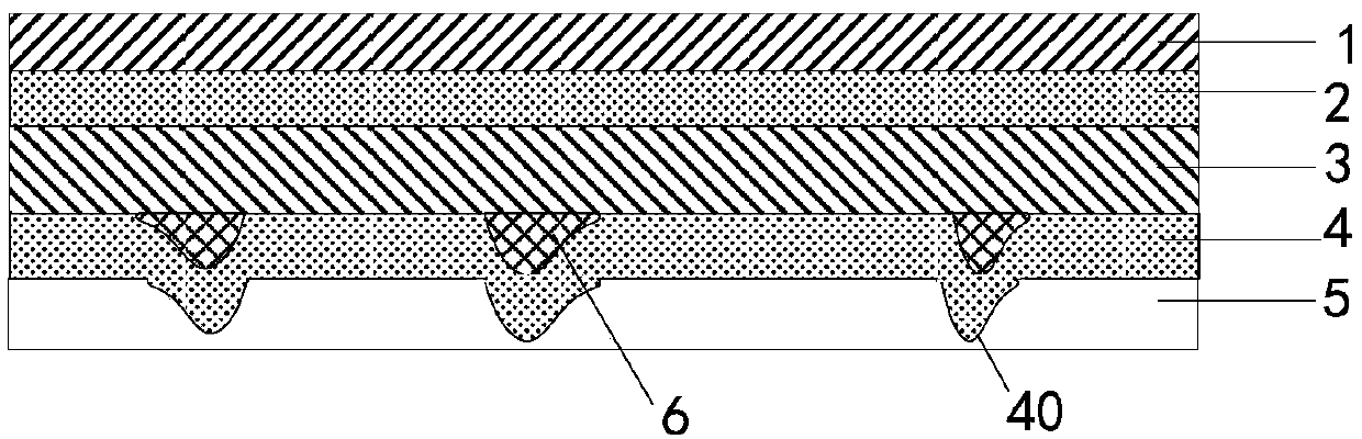
[0053] See figure 1 , the embodiment of the present invention provides an electromagnetic shielding film, which includes a first shielding layer 1, an adhesive layer 2, a second shielding layer 3, a third shielding layer 4 and an adhesive film layer 5; the first shielding layer 1 , the adhesive layer 2 and the second shielding layer 3 are stacked in sequence; the second shielding layer 3 is provided with a protrusion 6 on the side away from the adhesive layer 2; the third shielding layer 4 is provided on the side of the second shielding layer 3 where the protrusion is formed, and a protrusion 40 is formed on the position where the third shielding layer 4 covers the protrusion 6 (the protrusion 40 The relationship with the protrusions 6 can be one-to-one correspondence, one-to-many correspondence or multi-to-one correspondence, etc. When the relationship between the protrusions 40 and the protrusions 6 is one-to-one correspondence, the protrusions 40 The shape and structure of...

Embodiment 2

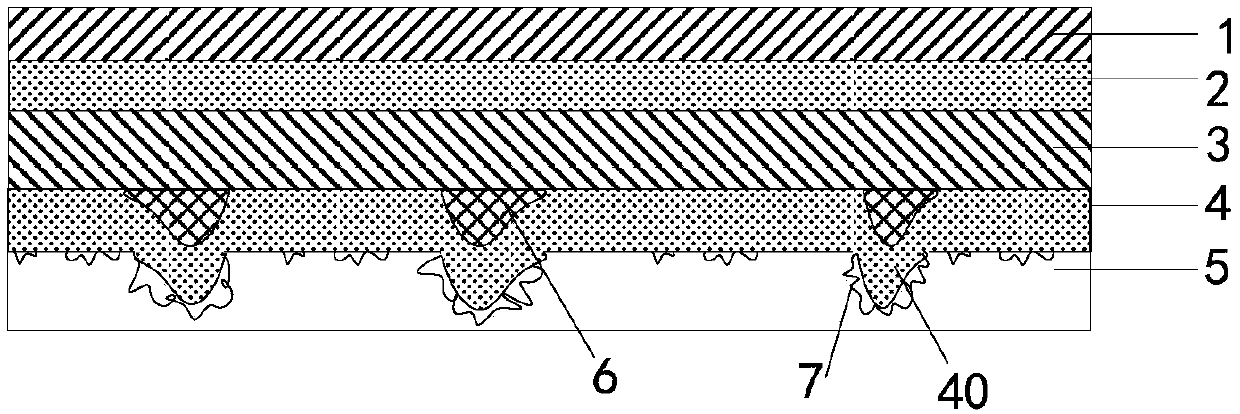
[0072] See figure 2 , the present embodiment provides another electromagnetic shielding film, which differs from the first embodiment mainly in that a plurality of conductor particles 7 are provided on the surface of the raised portion 40 . Wherein, by arranging the conductor particles 7 on the surface of the raised portion 40, it is further ensured that the raised portion 40 can ensure that the third shielding layer 4 can smoothly penetrate the adhesive film during the pressing process. Layer 5, thereby ensuring the normal export of disturbing charges.

[0073] Preferably, the diameter of the conductor particles 7 is 0.1 μm-30 μm.

[0074] Preferably, the conductive particles 7 are concentrated and distributed on the protruding positions on the surface of the raised portion 40 , so that it is easier to pierce the adhesive film layer 5 . Certainly, the non-convex portion on the surface of the protruding portion 40 may also have conductor particles 7 distributed therein. In...

Embodiment 3

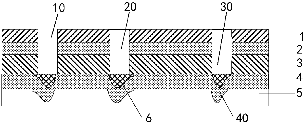
[0079] See image 3 and Figure 5 , this embodiment provides another electromagnetic shielding film, which differs from Embodiment 1 and Embodiment 2 mainly in that: the first through hole 10 is provided on the first shielding layer 1 through its upper and lower surfaces, and the The second shielding layer 3 is provided with a second through hole 30 passing through its upper and lower surfaces, and the adhesive layer 2 is provided with a third through hole 20 passing through its upper and lower surfaces; the outer side of each second through hole 30 The protrusion 6 is correspondingly formed at the position; the protrusion 6 is solidified when the fluid resin flows from the first through hole 10 to the outside of the second through hole 30 through the third through hole 20 Formed; wherein, the outer side of the second through hole 30 is away from the adhesive layer 2 .

[0080] Preferably, the first through hole 10, the second through hole 30 and the third through hole 20 ar...


PUM

PropertyMeasurementUnit
thicknessaaaaaaaaaa
diameteraaaaaaaaaa

Abstract

The invention discloses an electromagnetic interference (EMI) shielding film, a circuit board and a preparation method of the EMI shielding film. The EMI shielding film comprises a first shielding layer, a bonding layer, a second shielding layer, a third shielding layer and an adhesive film layer, wherein the first shielding layer, the bonding layer and the second shielding layer are arranged sequentially in a stacked mode; bulges are arranged on the side, away from the bonding layer, of the second shielding layer; the third shielding layer is arranged on the side, provided with the bulges, ofthe second shielding layer, and protruding parts are formed at positions, covering the bulges, of the third shielding layer; and the adhesive film layer is arranged on the side, away from the secondshielding layer, of the third shielding layer in a covering mode. According to the EMI shielding film, the protruding parts extend into the adhesive film layer, so that when the protruding parts are press-fitted, it is guaranteed that the third shielding layer smoothly pierces through the adhesive film layer to make contact with a ground layer of the circuit board; and then, it is guaranteed thatinterference charges are normally led out under cooperation of the first shielding layer, the bonding layer, the second shielding layer and the third shielding layer, and a shielding function is achieved.

Description

technical field [0001] The invention relates to the field of electronics, in particular to an electromagnetic shielding film, a circuit board and a preparation method of the electromagnetic shielding film. Background technique [0002] With the rapid development of the electronics industry, electronic products are further developed toward miniaturization, light weight, and high-density assembly, which greatly promotes the development of flexible circuit boards, thereby realizing the integration of component devices and wire connections. Flexible circuit boards can be widely used in industries such as mobile phones, liquid crystal displays, communications and aerospace. [0003] Driven by the international market, functional flexible circuit boards dominate the flexible circuit board market, and an important indicator for evaluating the performance of functional flexible circuit boards is electromagnetic shielding (Electromagnetic Interference Shielding, referred to as EMI Sh...

Claims


Application Information

Patent Timeline
Patent Type & Authority Applications(China)
IPC IPC(8): H05K9/00B32B33/00B32B3/08
CPCH05K9/0088B32B33/00B32B3/08B32B2307/212B32B2457/08
Inventor 苏陟
Owner GUANGZHOU FANGBANG ELECTRONICS
Why Eureka
Try Eureka