Bearing device, process chamber and semiconductor processing equipment

A technology for carrying devices and semiconductors, which is used in semiconductor/solid-state device manufacturing, electrical components, circuits, etc., and can solve problems such as uneven force on wafers, wafer scratches, and losses.

Active Publication Date: 2020-02-14
BEIJING NAURA MICROELECTRONICS EQUIP CO LTD
View PDF4 Cites 1 Cited by
  • Summary
  • Abstract
  • Description
  • Claims
  • Application Information

AI Technical Summary

Problems solved by technology

[0003] However, in the above-mentioned structure, the wafer is lifted up directly by using the lifting pin, and the lifting pin is in local point contact with the wafer. The pin-up method will cause uneven force on the wafer

Method used


Image

  • Bearing device, process chamber and semiconductor processing equipment
  • Bearing device, process chamber and semiconductor processing equipment
  • Bearing device, process chamber and semiconductor processing equipment

Examples


Embodiment Construction

[0049] Specific embodiments of the present invention will be described in detail below in conjunction with the accompanying drawings. It should be understood that the specific embodiments described here are only used to illustrate and explain the present invention, and are not intended to limit the present invention.

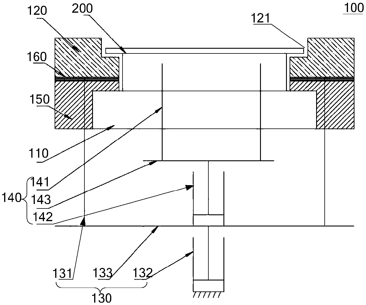
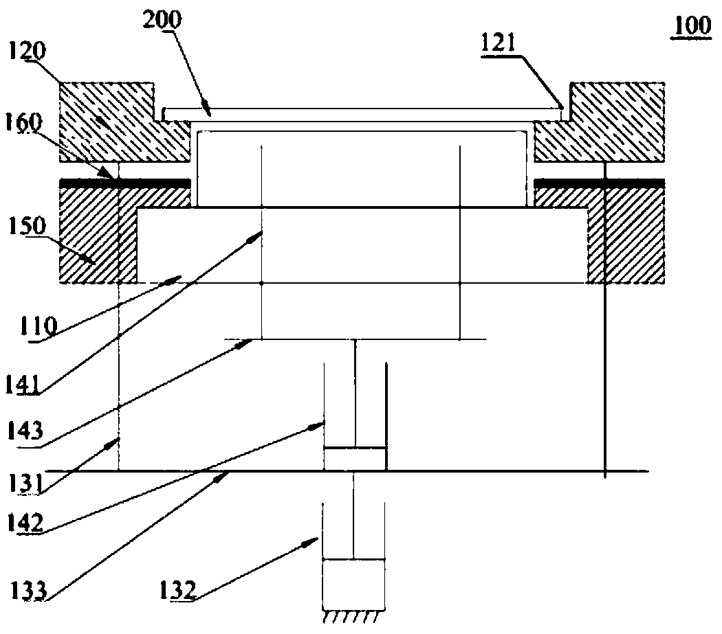
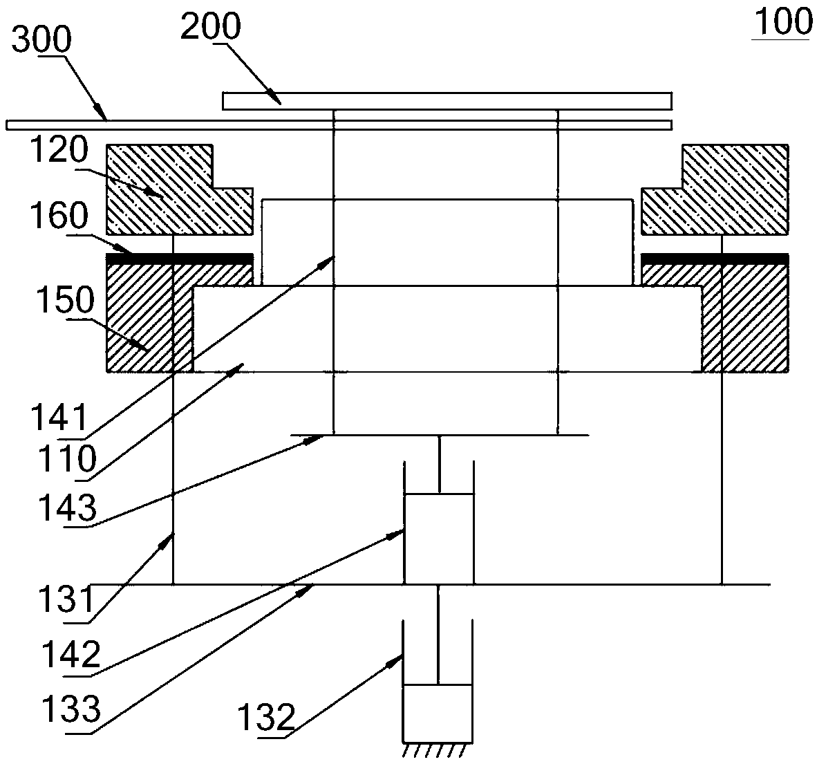
[0050] Such as Figure 1 to Figure 5 As shown, the first aspect of the present invention relates to a carrier device 100, which includes an electrostatic chuck 110, a support ring 120, a first drive assembly 130, a second drive assembly 140, and the like.

[0051] Among them, such as figure 1 As shown, the support ring 120 is arranged around the circumferential side wall of the electrostatic chuck 110, and the support ring 120 and the electrostatic chuck 110 jointly support the workpiece 200 to be processed. The workpiece 200 to be processed depends on the specific application scenario, for example, In the field of semiconductor manufacturing, the workpiece 20...


PUM


Abstract

The invention discloses a bearing device, a process chamber and semiconductor processing equipment. The bearing device comprises an electrostatic chuck and a supporting ring arranged around the circumferential side wall of the electrostatic chuck, wherein the electrostatic chuck and the supporting ring jointly bear a to-be-machined part. The bearing device further comprises a first driving assembly and a second driving assembly, wherein the first driving assembly is used for driving the supporting ring to move to a first unloading position so as to separate the to-be-machined part from the electrostatic chuck; and the second driving assembly is used for driving the to-be-machined part to move to a second unloading position so as to separate the to-be-machined part is separated from the supporting ring. When the supporting ring jacks up the to-be-machined part, the supporting ring is in uniform annular surface contact with the to-be-machined part, the phenomenon that the to-be-machinedpart is uneven in stress due to piece sticking and the like can be avoided. In addition, when the to-be-machined part is jacked up by the second driving assembly, only the weight of the to-be-machinedpart needs to be overcome, and thus the phenomenon that the to-be-machined part deviates is avoided.

Description

technical field [0001] The present invention relates to the technical field of semiconductor manufacturing, in particular to a carrying device, a process chamber including the carrying device, and semiconductor processing equipment including the process chamber. Background technique [0002] Generally, after the wafer enters the process chamber, the electrostatic chuck uses a high-voltage DC voltage to adsorb and fix the wafer, and then the wafer undergoes a process. After the process is completed, the electrostatic chuck applies a reverse high-voltage DC voltage to the wafer. The wafer is dechucked, and then the needle is lifted to separate the wafer from the electrostatic chuck, and finally passed out of the chamber by the robot. [0003] However, in the above-mentioned structure, the wafer is lifted up directly by using the lifting pin, and the lifting pin is in local point contact with the wafer. The pin-up method will cause uneven force on the wafer, resulting in offse...

Claims


Application Information

Patent Timeline
IPC IPC(8): H01L21/683
CPCH01L21/6831H01L21/6833
Inventor 李华
Owner BEIJING NAURA MICROELECTRONICS EQUIP CO LTD
Why Eureka
Try Eureka