Wafer defect scanning method

A defect scanning and wafer technology, applied in electrical components, circuits, semiconductor/solid-state device testing/measurement, etc., to solve the problem that wafer defects cannot be detected in time

Active Publication Date: 2020-03-06
SHANGHAI HUALI MICROELECTRONICS CORP
View PDF7 Cites 2 Cited by
  • Summary
  • Abstract
  • Description
  • Claims
  • Application Information

AI Technical Summary

Problems solved by technology

[0004] The object of the present invention is to provide a wafer defect scanning method to solve t

Method used


Image

  • Wafer defect scanning method
  • Wafer defect scanning method
  • Wafer defect scanning method

Examples


Embodiment Construction

[0025] The wafer defect scanning method proposed by the present invention will be further described in detail below in conjunction with the accompanying drawings and specific embodiments. The advantages and features of the present invention will become clearer from the following description. It should be noted that all the drawings are in a very simplified form and use imprecise scales, and are only used to facilitate and clearly assist the purpose of illustrating the embodiments of the present invention. In addition, the structures shown in the drawings are often a part of the actual structure. In particular, each drawing needs to display different emphases, and sometimes uses different scales.

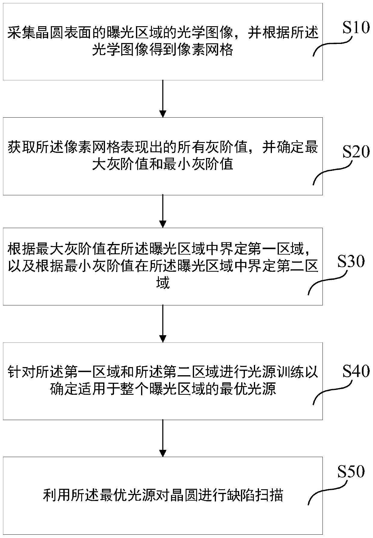
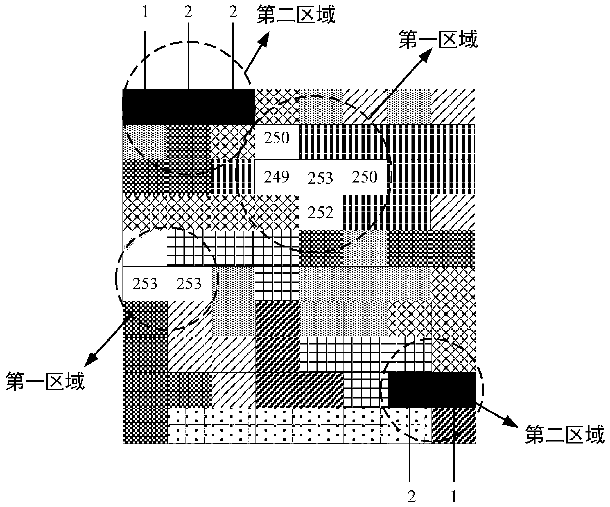
[0026] The present invention provides a wafer defect scanning method, referring to figure 1 , figure 1 It is a flowchart of a wafer defect scanning method according to an embodiment of the present invention, and the wafer defect scanning method includes:

[0027] S10: collecting ...


PUM


Abstract

The invention provides a wafer defect scanning method, which includes: acquiring an optical image of a wafer, and obtaining a pixel grid according to the optical image; obtaining all grayscale valuesof the pixel grid, and determining a maximum grayscale value and a minimum grayscale value; delimiting a first area in an exposure area according to the maximum grayscale value, and delimiting a second area in the exposure area according to the minimum grayscale value; for the first area and the second area, training a light source to determine an optimal light source suitable for the entire exposure area; and scanning the defects of the wafer by using the optimal light source. The method selects out the first area by using the maximum grayscale value and selects out the second area by using the minimum grayscale value, avoids a mistake caused by manually selecting the first area and the second area so as to improve the accuracy of configuring the light source suitable for the entire exposure area, and contributes to the observation of the wafer defects so that the defects on the wafer surface can be detected in time.

Description

technical field [0001] The invention relates to the technical field of semiconductor manufacturing, in particular to a wafer defect scanning method. Background technique [0002] With the further development of semiconductor technology, wafer defect scanning has become an indispensable means to improve semiconductor yield, so the establishment of defect scanning process program is very important. [0003] Wafer defect scanning needs to be completed using defect scanning machines. The establishment of scanning process programs in defect scanning machines is usually done manually. Among them, light source training (light source configuration) plays a crucial role in defect scanning process programs. The current wafer defect scanning method usually uses human judgment, selects the brightest and darkest areas on the wafer surface, and conducts light source training for the brightest and darkest areas to define the appropriate light source intensity, so that the definition is app...

Claims


Application Information

Patent Timeline
IPC IPC(8): H01L21/66
CPCH01L22/12
Inventor 韩俊伟
Owner SHANGHAI HUALI MICROELECTRONICS CORP
Why Eureka
Try Eureka