OLED light-emitting panel
A technology of light-emitting panel and light-emitting area, applied in the field of OLED, can solve the problems of lead occupied space and lead resistance, etc., and achieve the effect of improving the service life and reducing the array gap.
- Summary
- Abstract
- Description
- Claims
- Application Information
AI Technical Summary
Problems solved by technology
Method used
Image
Examples
Embodiment 1
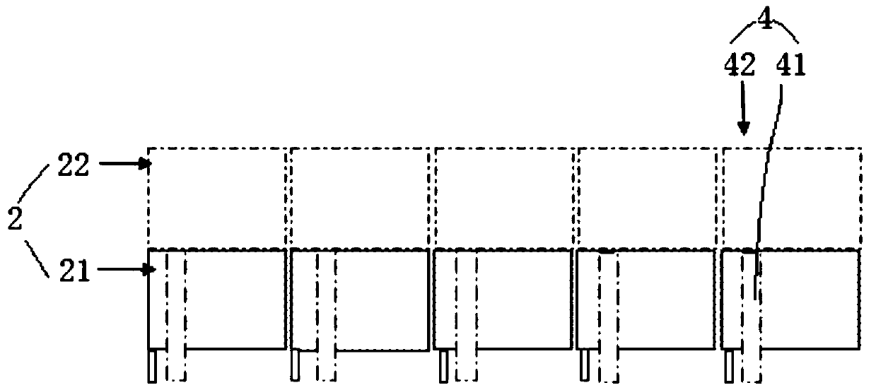
[0043] Such as figure 1 As shown, the OLED light-emitting panel provided by the present invention includes a substrate and a plurality of light-emitting regions 2 arranged in an array on the substrate. Each light-emitting region 2 is provided with a corresponding lead structure 4 electrically connected thereto. It includes a laminated lead layer 41 and an insulating layer 42 , the insulating layer 42 is disposed between two adjacent lead layers 41 , and each lead layer 41 is electrically connected to the corresponding light emitting area 2 after being led out. Here, the lead structure 4 is disposed on the back side of each light-emitting region 2 , and the lead structure 4 is distributed along the horizontal or vertical direction of the light-emitting regions 2 distributed in an array.
[0044] figure 1 There are 2 rows of light-emitting areas in the center, and there are 5 light-emitting areas in each row of light-emitting areas. All light-emitting areas can be seamlessly co...
Embodiment 2
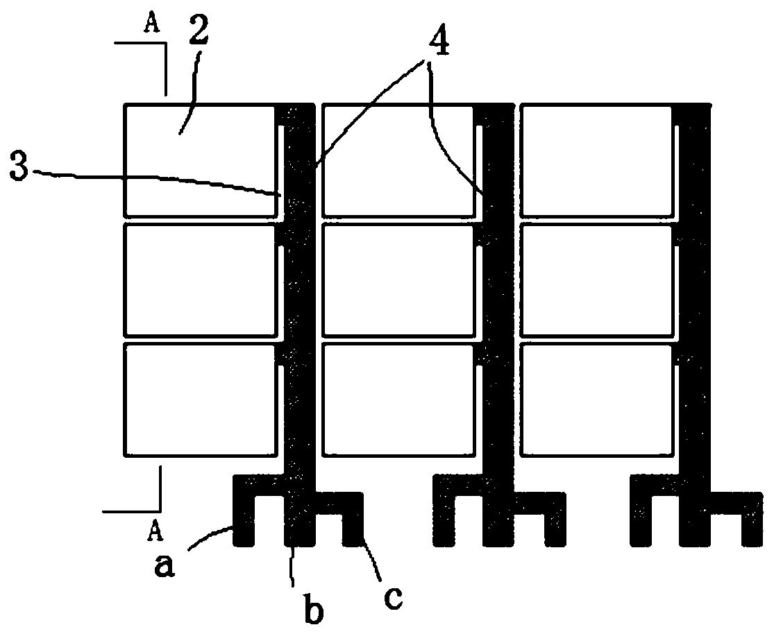
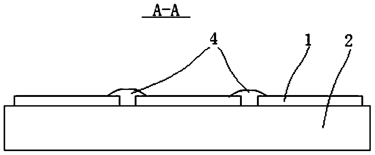
[0048] The OLED light-emitting panel provided in this embodiment includes a substrate 1 and a plurality of light-emitting regions 2 arranged in an array on the substrate 1, and array gaps 3 formed between the light-emitting regions 2 are provided with corresponding light-emitting regions 2. The electrode leads are lead structures 4 that are electrically connected. The lead structures 4 include stacked lead layers 41 and insulating layers 42. The insulating layer 42 is arranged between two adjacent lead layers 41. Each lead layer 41 is drawn out from the side and connected to the corresponding The light emitting regions 2 are electrically connected to each other.
[0049] For the case where the array gap is small, you can set as figure 2 and image 3 The structure shown in the figure realizes the three-dimensional structure of the lead, and all the lead layers are stacked together, for example, figure 2 A total of 9 light-emitting areas are set up to form a 3X3 array distri...
Embodiment 3
[0052] Such as Figure 4 As shown, the OLED light-emitting panel provided in this embodiment has a bottom-emitting structure, and the light-emitting area is further optimized on the basis of Example 2, and the three-dimensional light-emitting area is realized. Specifically, as Figure 5 As shown in the cross-sectional view, in the direction perpendicular to one side of the substrate 1, each row of light-emitting regions 2 is distributed in steps from one end of the substrate 1 to the other end, and two adjacent rows of light-emitting regions are separated by a transparent insulating layer.
[0053] The specific manufacturing process is: make the first row of light-emitting areas on the right end of the substrate, and make a lead layer electrically connected to each light-emitting area of the first row in the gap between the light-emitting areas of the first row, and then emit light in the first row Fabricate a transparent insulating layer on the substrate at the end of the ...
PUM
 Abstract
Description
Claims
Application Information


