Supercharge Your Innovation With Domain-Expert AI Agents!

Epitaxial substrate and manufacturing method thereof

A technology for epitaxial substrates and substrates, which is used in semiconductor/solid-state device manufacturing, semiconductor/solid-state device components, semiconductor devices, etc., and can solve the problems of immature Micro-LED display technology, small size of Micro-LED, and unfavorable alignment keys. Synthetic power, etc.

Active Publication Date: 2020-05-08
CHENGDU VISTAR OPTEOLECTRONICS CO LTD
View PDF8 Cites 1 Cited by
  • Summary
  • Abstract
  • Description
  • Claims
  • Application Information

AI Technical Summary

Problems solved by technology

[0003] Micro-LED (Micro Light Emitting Diode) display technology has the advantages of high brightness, high response speed, low power consumption, and long life, and has become a research hotspot for people to pursue a new generation of display technology. However, Micro-LED display The screen technology is still very immature, and many manufacturing technical problems still need to be solved
[0004] Due to the extremely small size of Micro-LED, the size of its electrode layer, passivation layer and other patterns is even smaller, which brings great challenges to the accuracy and process control of alignment bonding, which is not conducive to the success rate of alignment bonding

Method used


Image

  • Epitaxial substrate and manufacturing method thereof
  • Epitaxial substrate and manufacturing method thereof
  • Epitaxial substrate and manufacturing method thereof

Examples


Embodiment Construction

[0023] The following will clearly and completely describe the technical solutions in the embodiments of the present application with reference to the drawings in the embodiments of the present application. Obviously, the described embodiments are only some of the embodiments of the present application, not all of them. Based on the embodiments in this application, all other embodiments obtained by persons of ordinary skill in the art without making creative efforts belong to the scope of protection of this application.

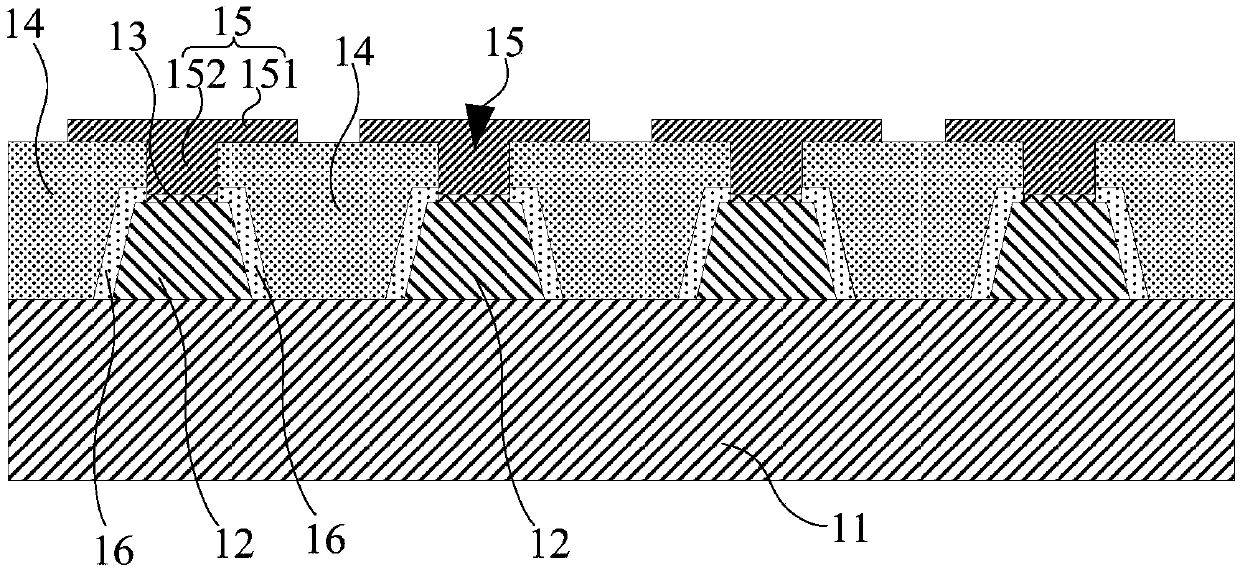
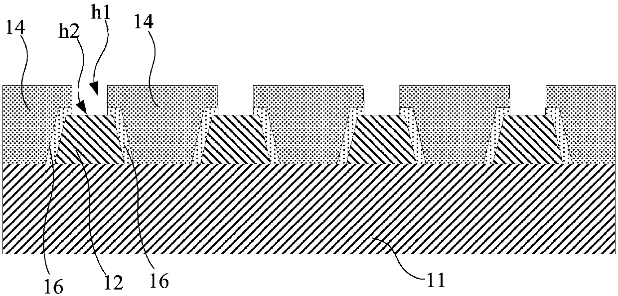
[0024] Please refer to figure 1 and figure 2 , figure 1 is a schematic structural view of the epitaxial substrate of the embodiment of the present application. figure 2 It is a structural schematic diagram of the epitaxial substrate of the embodiment of the present application after removing the pad and the contact electrode.

[0025] In this embodiment, the epitaxial substrate includes: a substrate body 11 , a plurality of bosses 12 , a plurality of cont...


PUM


Abstract

The invention discloses an epitaxial substrate. The epitaxial substrate comprises a substrate main body; a plurality of bosses which are arranged on the substrate main body in an array manner; a plurality of contact electrodes which are correspondingly arranged at the tops of the bosses, a planarization layer which covers the bosses and an area, which is not covered by the bosses, of the substratemain body, and a plurality of bonding pads which are arranged on the planarization layer in an array mode and are electrically connected to the corresponding contact electrodes through first throughholes, wherein the first through holes corresponding to the bosses are formed in the planarization layer so that the contact electrodes are exposed through the first through holes, and an area of thevertical projection of the bonding pads on the substrate main body is larger than that of the vertical projection of the contact electrodes on the substrate main body. The invention further disclosesa manufacturing method of the epitaxial substrate. In this way, the alignment success rate of the epitaxial substrate and a driving substrate can be increased.

Description

technical field [0001] The present application relates to the field of display technology, in particular to an epitaxial substrate and a manufacturing method thereof. Background technique [0002] In recent years, the semiconductor lighting technology has become more mature, the cost has been declining, and the industrial scale has become saturated, which provides a better light source for the development of LED display technology. [0003] Micro-LED (Micro Light Emitting Diode) display technology has the advantages of high brightness, high response speed, low power consumption, and long life, and has become a research hotspot for people to pursue a new generation of display technology. However, Micro-LED display The screen technology is still very immature, and many manufacturing technical problems still need to be solved. [0004] Due to the extremely small size of Micro-LED, the size of its electrode layer, passivation layer and other patterns is even smaller, which brin...

Claims


Application Information

Patent Timeline
Patent Type & Authority Applications(China)
IPC IPC(8): H01L23/13H01L23/488H01L21/48H01L21/50
CPCH01L23/488H01L23/13H01L21/48H01L21/50H01L33/62H01L25/0753H01L24/01H01L27/1214H01L33/32H01L33/44H01L33/52H01L2933/0025H01L2933/005H01L2933/0066
Inventor 郭恩卿邢汝博黄秀颀
Owner CHENGDU VISTAR OPTEOLECTRONICS CO LTD
Features
  • R&D
  • Intellectual Property
  • Life Sciences
  • Materials
  • Tech Scout
  • Unparalleled Data Quality
  • Higher Quality Content
  • 60% Fewer Hallucinations
Learn More