
Epitaxial substrate and manufacturing method thereof

一种外延基板、基板的技术,应用在半导体/固态器件制造、半导体/固态器件零部件、半导体器件等方向,能够解决不利对位键合成功率、Micro-LED显示屏技术不成熟、Micro-LED尺寸小等问题

Active Publication Date: 2022-03-22
CHENGDU VISTAR OPTEOLECTRONICS CO LTD
View PDF8 Cites 0 Cited by
  • Summary
  • Abstract
  • Description
  • Claims
  • Application Information

AI Technical Summary

Problems solved by technology

[0003] Micro-LED (Micro Light Emitting Diode) display technology has the advantages of high brightness, high response speed, low power consumption, and long life, and has become a research hotspot for people to pursue a new generation of display technology. However, Micro-LED display The screen technology is still very immature, and many manufacturing technical problems still need to be solved
[0004] Due to the extremely small size of Micro-LED, the size of its electrode layer, passivation layer and other patterns is even smaller, which brings great challenges to the accuracy and process control of alignment bonding, which is not conducive to the success rate of alignment bonding

Method used


Image

  • Epitaxial substrate and manufacturing method thereof
  • Epitaxial substrate and manufacturing method thereof
  • Epitaxial substrate and manufacturing method thereof

Examples


Embodiment Construction

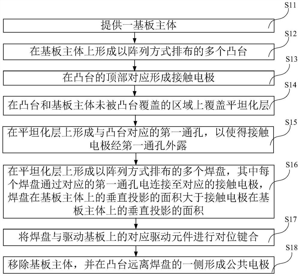
[0023] The following will clearly and completely describe the technical solutions in the embodiments of the present application with reference to the drawings in the embodiments of the present application. Obviously, the described embodiments are only some of the embodiments of the present application, not all of them. Based on the embodiments in this application, all other embodiments obtained by persons of ordinary skill in the art without making creative efforts belong to the scope of protection of this application.

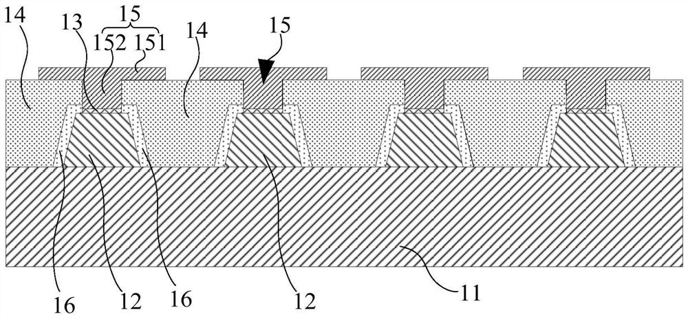
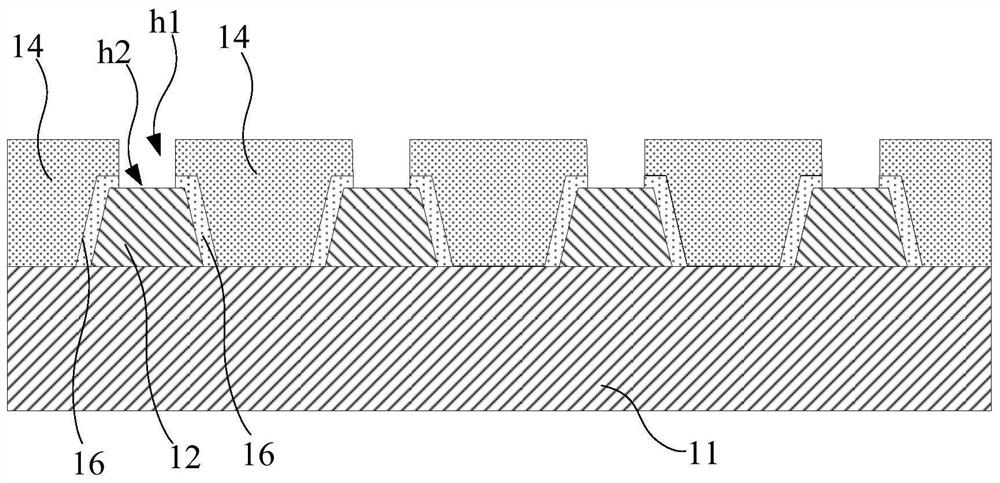
[0024] Please refer to figure 1 with figure 2 , figure 1 is a schematic structural view of the epitaxial substrate of the embodiment of the present application. figure 2 It is a structural schematic diagram of the epitaxial substrate of the embodiment of the present application after removing the pad and the contact electrode.

[0025] In this embodiment, the epitaxial substrate includes: a substrate body 11 , a plurality of bosses 12 , a plurality of con...


PUM


Abstract

The application discloses an epitaxial substrate, which includes: a substrate body; a plurality of bosses arranged on the substrate body in an array; a plurality of contact electrodes correspondingly arranged on the top of the bosses; a planarization layer covering On the area where the boss and the substrate body are not covered by the boss, the planarization layer is provided with a first through hole corresponding to the boss, so that the contact electrode is exposed through the first through hole; a plurality of pads are arranged in an array arranged on the planarization layer and electrically connected to the corresponding contact electrode through the first through hole, wherein the area of ​​the vertical projection of the pad on the substrate body is larger than the area of ​​the vertical projection of the contact electrode on the substrate body. The application also discloses a method for manufacturing the epitaxial substrate. Through the above method, the present application can improve the alignment success rate of the epitaxial substrate and the driving substrate.

Description

technical field [0001] The present application relates to the field of display technology, in particular to an epitaxial substrate and a manufacturing method thereof. Background technique [0002] In recent years, the semiconductor lighting technology has become more mature, the cost has been declining, and the industrial scale has become saturated, which provides a better light source for the development of LED display technology. [0003] Micro-LED (Micro Light Emitting Diode) display technology has the advantages of high brightness, high response speed, low power consumption, and long life, and has become a research hotspot for people to pursue a new generation of display technology. However, Micro-LED display The screen technology is still very immature, and many manufacturing technical problems still need to be solved. [0004] Due to the extremely small size of Micro-LED, the size of its electrode layer, passivation layer and other patterns is even smaller, which brin...

Claims


Application Information

Patent Timeline
Patent Type & Authority Patents(China)
IPC IPC(8): H01L23/13H01L23/488H01L21/48H01L21/50
CPCH01L23/488H01L23/13H01L21/48H01L21/50H01L33/62H01L25/0753H01L24/01H01L27/1214H01L33/32H01L33/44H01L33/52H01L2933/0025H01L2933/005H01L2933/0066
Inventor 郭恩卿邢汝博黄秀颀
Owner CHENGDU VISTAR OPTEOLECTRONICS CO LTD
Learn More