Display panel compensation circuit structure and display device

A display panel and compensation circuit technology, applied to static indicators, instruments, etc., can solve the problems of long reading time of demura data, achieve the effects of improving user experience, fast reading, and increasing compensation speed

Active Publication Date: 2020-06-19
TCL CHINA STAR OPTOELECTRONICS TECH CO LTD
View PDF5 Cites 0 Cited by
  • Summary
  • Abstract
  • Description
  • Claims
  • Application Information

AI Technical Summary

Problems solved by technology

However, as the resolution of the panel becomes larger and larger, the reading time for the logic control board to read the demura data is getting longer and longer.

Method used


Image

  • Display panel compensation circuit structure and display device
  • Display panel compensation circuit structure and display device
  • Display panel compensation circuit structure and display device

Examples


Embodiment Construction

[0029] The technical solutions in the embodiments of the present application will be clearly and completely described below in conjunction with the drawings in the embodiments of the present application. Apparently, the described embodiments are only some of the embodiments of this application, not all of them. Based on the embodiments in this application, all other embodiments obtained by those skilled in the art without making creative efforts belong to the scope of protection of this application.

[0030] It should be noted that like numerals and letters denote similar items in the following figures, therefore, once an item is defined in one figure, it does not require further definition and explanation in subsequent figures. Meanwhile, in the description of the present application, the terms "first", "second" and the like are only used to distinguish descriptions, and cannot be understood as indicating or implying relative importance.

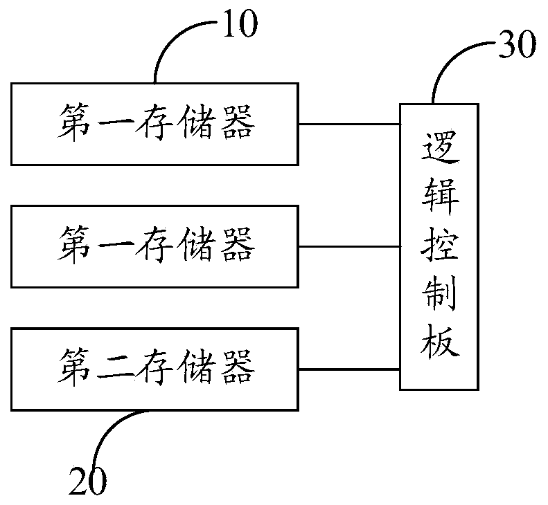
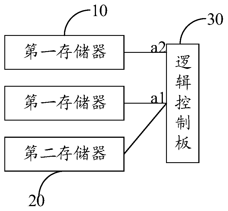
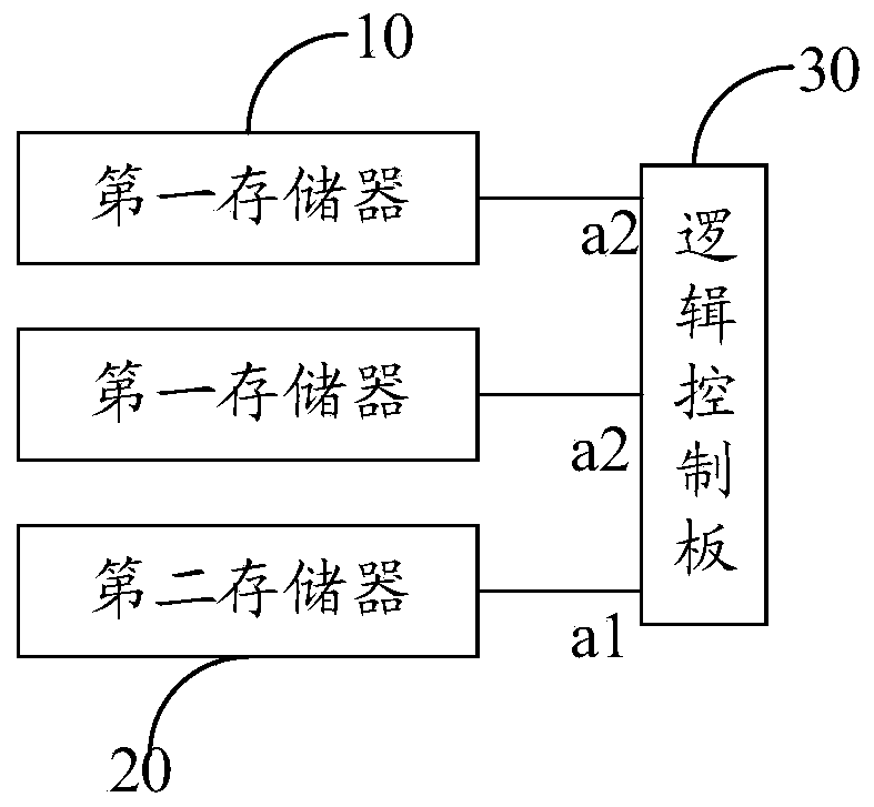
[0031] Please refer to figure 1 , ...


PUM


Abstract

The embodiment of the invention provides a display panel compensation circuit structure and a display device. The display panel compensation circuit structure comprises at least two first storages, atleast two second storages, at least two third storages, at least two fourth storages, at least two fifth storages and at least two sixth storages, the second memory is used for storing the distribution information of the Demura data in at least two first memories; and the logic control panel is used for simultaneously reading the corresponding Demura data from the at least two first memories according to the distribution information so as to compensate the display panel. According to the embodiment of the invention, the method can improve the compensation speed through achieving the quick reading of the Demura data, and can improve the user experience.

Description

technical field [0001] The present application relates to the field of display technology, in particular, to a display panel compensation circuit structure and a display device. Background technique [0002] With the increasing size of display panels, many panel makers are currently developing 55-inch to 85-inch panels, and the resolution is getting higher and higher. From HD to FHD and UD, now to 8K resolution. Because, during the manufacturing process of the display panel, based on various manufacturing processes or unfavorable factors that need splicing of large-size panels, it may cause bad mura phenomenon on the panel. At present, many panel factories will do mura in the production process of the panel. compensation. The method is to take pictures with a precision camera and then generate the mura compensation table through algorithm processing, and then burn the mura compensation table into the memory on the panel. When the logic control board is powered on, it will ...

Claims


Application Information

Patent Timeline
Patent Type & Authority Applications(China)
IPC IPC(8): G09G3/20
CPCG09G3/20Y02D10/00
Inventor 童焕勋
Owner TCL CHINA STAR OPTOELECTRONICS TECH CO LTD
Why Eureka
Try Eureka