Display substrate, manufacturing method thereof, and display device

A technology for displaying substrates and display areas, applied in instruments, semiconductor devices, computing, etc., can solve problems such as the influence of wiring reliability, and achieve the effect of improving reliability and reducing climbing height

Active Publication Date: 2022-01-11
BOE TECH GRP CO LTD +1
View PDF0 Cites 0 Cited by
  • Summary
  • Abstract
  • Description
  • Claims
  • Application Information

AI Technical Summary

Problems solved by technology

[0004] Embodiments of the present invention provide a display substrate, a manufacturing method thereof, and a display device, so as to solve the problem that the blocking structure may affect the reliability of wiring

Method used


Image

  • Display substrate, manufacturing method thereof, and display device
  • Display substrate, manufacturing method thereof, and display device
  • Display substrate, manufacturing method thereof, and display device

Examples


Embodiment Construction

[0033] The following will clearly and completely describe the technical solutions in the embodiments of the present invention with reference to the accompanying drawings in the embodiments of the present invention. Obviously, the described embodiments are some of the embodiments of the present invention, but not all of them. Based on the embodiments of the present invention, all other embodiments obtained by persons of ordinary skill in the art without creative efforts fall within the protection scope of the present invention.

[0034] An embodiment of the present invention provides a display substrate.

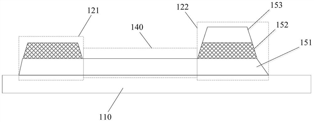
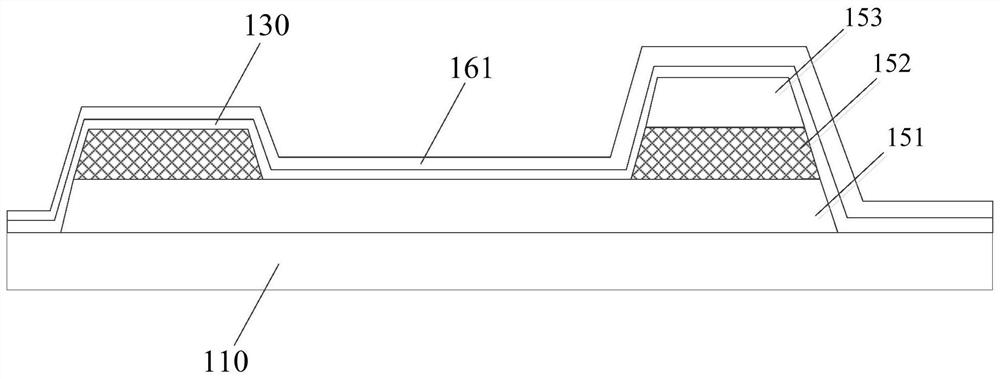
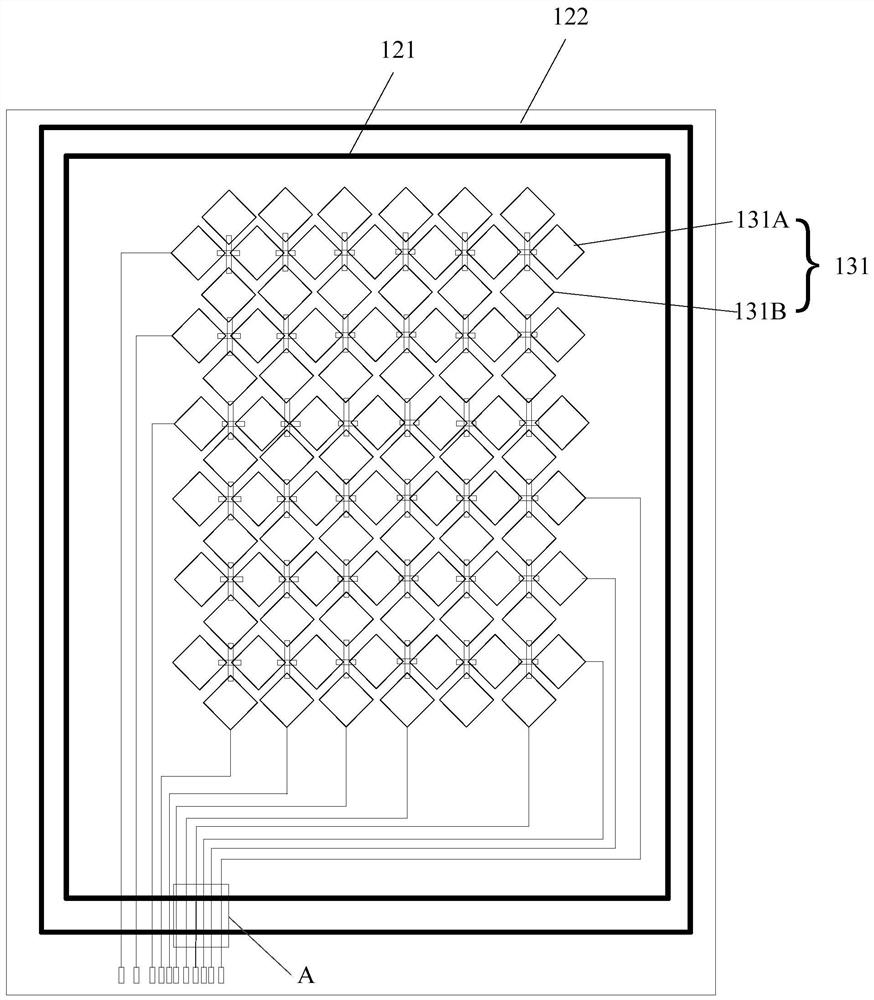
[0035] In one embodiment, the display substrate includes a base substrate 110 and a light-emitting layer on the base substrate 110, which may also include some other functional film layers. For details, please refer to the display substrate in the related art, which will not be further described here. Qualify and describe.

[0036] Such as Figure 1A with Figure 1B As show...


PUM


Abstract

The invention provides a display substrate, a manufacturing method thereof, and a display device. The display substrate includes a base substrate, a display area, a peripheral area surrounding the display area, touch electrodes, touch electrode lines, and a first barrier structure and a second barrier structure located in the peripheral area, and the first barrier structure is arranged around the display area , the second barrier structure surrounds the first barrier structure and is spaced apart from the first barrier structure; and the touch electrode line extends from the display area to the peripheral area of ​​the second barrier structure away from the display area; it is located between the first barrier structure and the second barrier structure The minimum value of the vertical distance between the touch electrode line and the base substrate between the two barrier structures is greater than the vertical distance between the surface of the first barrier structure and the second barrier structure near the base substrate and the base substrate minimum value. In this way, the embodiment of the present invention can reduce the climbing height during the routing of the conductive layer, thereby helping to improve the reliability of the routing.

Description

technical field [0001] The invention relates to the field of display technology, in particular to a display substrate, a manufacturing method thereof, and a display device. Background technique [0002] The light-emitting unit of an OLED (Organic Light Emitting Diode, Organic Light Emitting Diode) display device usually includes a first inorganic layer, an organic light-emitting layer and a second inorganic layer that are stacked. It may invade along the interface of the film layer and cause damage to the organic light-emitting layer. The OLED display panel in the related art generally uses a raised barrier structure (dam) around the display area to improve the water / oxygen barrier, which can significantly improve the water / oxygen barrier effect. [0003] However, some traces of the display panel need to cross these barrier structures. For example, for a display panel with on-cell touch sensors integrated with pixel units, the traces of the touch sensor need to cross the ba...

Claims


Application Information

Patent Timeline
Patent Type & Authority Patents(China)
IPC IPC(8): G06F3/041H01L27/32
CPCG06F3/0412G06F2203/04103H10K59/40H10K59/12H10K59/1201G06F3/04164G06F3/0445G06F2203/04111H10K50/844H10K71/00
Inventor 刘阳升胡许武林伟金楻
Owner BOE TECH GRP CO LTD
Why Eureka
Try Eureka