Array substrate, display panel and display device

An array substrate and substrate substrate technology, which is applied to semiconductor devices, electrical components, circuits, etc., can solve the problems of limiting the aperture ratio of high PPI display panels, reducing the yield of array substrates, and data line climbing and disconnection, etc. The effect of poor line breakage, reduced climbing height, and improved yield

Active Publication Date: 2020-01-10
BOE TECH GRP CO LTD +1
View PDF5 Cites 0 Cited by
  • Summary
  • Abstract
  • Description
  • Claims
  • Application Information

AI Technical Summary

Problems solved by technology

[0002] High PPI (Pixels Per Inch) design is an important development trend of display panels, but the line width of the data lines on the display panel limits the aperture ratio of high PPI display panels
The thinner design of the data line is beneficial to the guarantee of the aperture ratio of the high PPI display panel, but the subsequent step open of the data line is the main problem faced in the process
[0003] Please refer to figure 1 , figure 1 It is a schematic cross-sectional structure diagram of an array substrate in the prior art, the array substrate includes a base substrate 11, and a gate metal layer pattern 12, a gate insulating layer 13 and a source-drain metal layer pattern 14 arranged on the base substrate 11, The gate metal layer pattern 12 includes gate lines, and the source-drain metal layer pattern 14 includes data lines. Due to the thinning of the data lines, it is easy for the data line to climb and break at the position where the data line crosses the gate line, thereby causing the yield rate of the array substrate to decrease. reduce

Method used


Image

  • Array substrate, display panel and display device
  • Array substrate, display panel and display device
  • Array substrate, display panel and display device

Examples


Embodiment Construction

[0022] In order to make the purpose, technical solutions and advantages of the embodiments of the present invention more clear, the following will clearly and completely describe the technical solutions of the embodiments of the present invention in conjunction with the drawings of the embodiments of the present invention. Apparently, the described embodiments are some, not all, embodiments of the present invention. All other embodiments obtained by those skilled in the art based on the described embodiments of the present invention belong to the protection scope of the present invention.

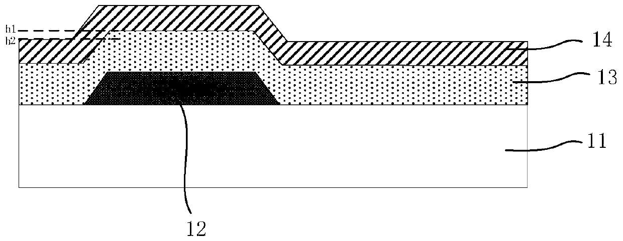
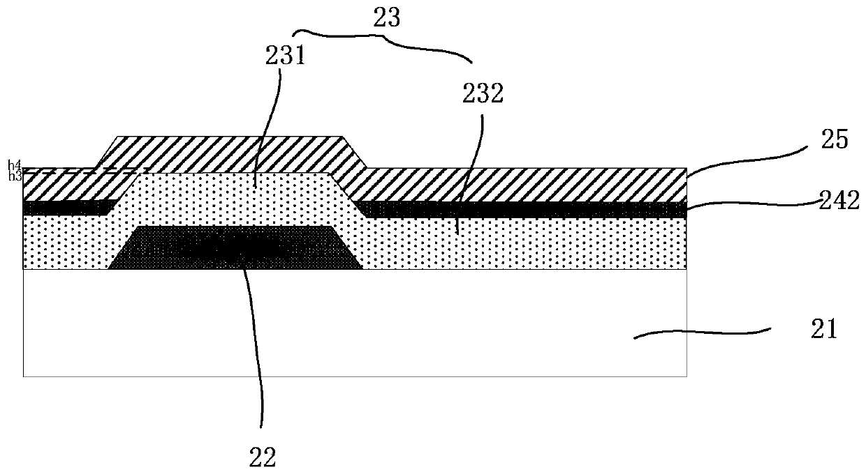
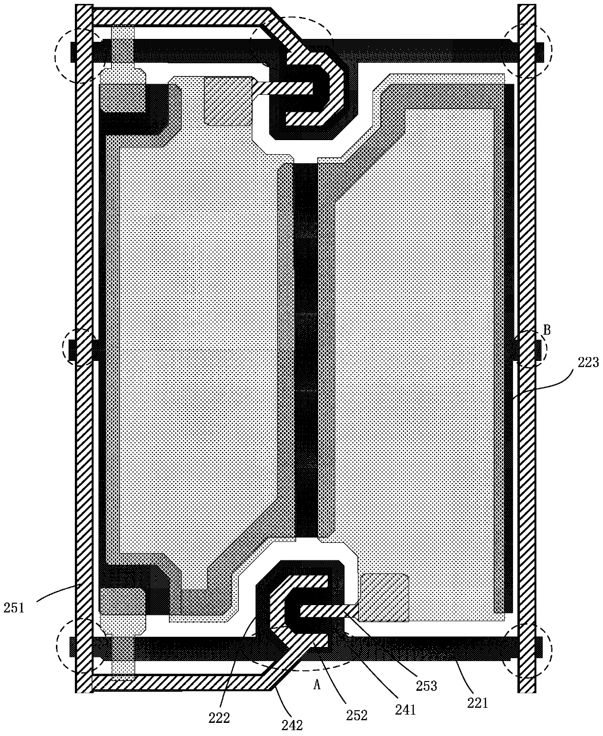
[0023] An embodiment of the present invention provides an array substrate, including a base substrate and a gate metal layer pattern, a gate insulating layer, and a source-drain metal layer pattern sequentially arranged on the base substrate, and the source-drain metal layer pattern has For the part of the gate metal layer pattern, the array substrate further includes: a climbing auxiliary ...


PUM


Abstract

The invention provides an array substrate, a display panel and a display device. The array substrate comprises a base substrate, and a gate metal layer pattern, a gate insulating layer and a source-drain metal layer pattern which are sequentially arranged on the base substrate, wherein the source-drain metal layer pattern has a part spanning the gate metal layer pattern; the array substrate also comprises a climbing assistance layer used for reducing the climbing height at the position where the source-drain metal layer pattern spans the gate metal layer pattern. The array substrate can effectively solve the problem of climbing disconnection of the source-drain metal layer pattern; the yield of array substrates is increased.

Description

technical field [0001] The present invention relates to the field of display technology, in particular to an array substrate, a display panel and a display device. Background technique [0002] High PPI (Pixels Per Inch) design is an important development trend of the display panel, but the line width of the data lines on the display panel limits the aperture ratio of the high PPI display panel. The thinner design of the data line is beneficial to guarantee the aperture ratio of the high PPI display panel, but the subsequent step open of the data line is the main problem faced in the process. [0003] Please refer to figure 1 , figure 1 It is a schematic cross-sectional structure diagram of an array substrate in the prior art, the array substrate includes a base substrate 11, and a gate metal layer pattern 12, a gate insulating layer 13 and a source-drain metal layer pattern 14 arranged on the base substrate 11, The gate metal layer pattern 12 includes gate lines, and the...

Claims


Application Information

Patent Timeline
Patent Type & Authority Patents(China)
IPC IPC(8): H01L27/12
CPCH01L27/1244
Inventor 刘珠林汪锐王孝林吴君辉熊兴夏炎
Owner BOE TECH GRP CO LTD
Why Eureka
Try Eureka