A display panel, its manufacturing method and display device

A technology for a display panel and a display device, applied in the field of display panel, display device and their preparation, can solve the problems of uneven film thickness of the light-emitting layer, affecting the display effect, etc.

Active Publication Date: 2019-08-13
HEFEI XINSHENG OPTOELECTRONICS TECH CO LTD +1
View PDF3 Cites 0 Cited by
  • Summary
  • Abstract
  • Description
  • Claims
  • Application Information

AI Technical Summary

Problems solved by technology

[0006] Embodiments of the present invention provide a display panel and a preparation method thereof, which are used to solve the problem in the prior art that the display effect of the display panel is affected by the uneven film thickness of the light-emitting layer formed due to the climbing of ink droplets

Method used


Image

  • A display panel, its manufacturing method and display device
  • A display panel, its manufacturing method and display device
  • A display panel, its manufacturing method and display device

Examples


preparation example Construction

[0050] Based on the same inventive concept, an embodiment of the present invention also provides a method for manufacturing a display panel, such as Figure 4 shown, including:

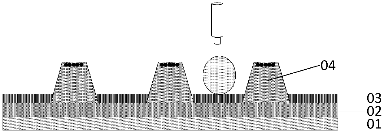
[0051] S401, forming a pattern of a plurality of anodes arranged in a matrix on the base substrate;

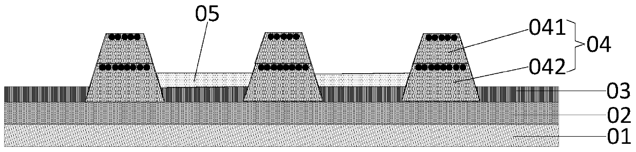
[0052] S402, forming a pattern of a first pixel defining layer between each anode on the base substrate formed with each anode; wherein the upper surface of the first pixel defining layer has liquid repellency;

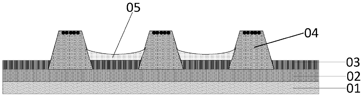
[0053] S403, forming a pattern of a second pixel defining layer on a side of the first pixel defining layer facing away from the base substrate; wherein the upper surface of the second pixel defining layer has liquid repellency.

[0054] The above-mentioned display panel manufacturing method provided by the embodiment of the present invention divides the existing pixel defining layer into two layers, that is, the pixel defining layer includes a first pixel defining layer and a second pixel d...


PUM


Abstract

The present invention provides a display panel, its preparation method and a display device. By dividing the pixel defining layer into a two-layer structure, and the upper surface of the two-layer structure has liquid repellency, the material containing the light-emitting layer is subsequently sprayed by an inkjet printing process. When the ink is used, because the upper surface of the first pixel defining layer has liquid repellency, it blocks the climbing of the ink drop to the second pixel defining layer, reduces the climbing height of the ink drop, and makes the film thickness of the formed luminescent layer more uniform; Because the remaining part of the second pixel defining layer except the upper surface has lyophilicity, ink droplets comprising the material of the light emitting layer will remain on the side of the second pixel defining layer close to the light emitting layer, because the upper surface of the first pixel defining layer has a Liquid repellency, which inhibits the climbing of the light-emitting layer before drying and forming a film, and ensures the uniformity of the film interface; at the same time, the light-emitting film remaining on the side wall of the second pixel boundary layer is physically disconnected from the light-emitting layer, ensuring that the remaining The film layer on the sidewall of the second pixel defining layer will not affect the luminous characteristics of the panel.

Description

technical field [0001] The invention relates to the field of display technology, in particular to a display panel, a preparation method thereof and a display device. Background technique [0002] Compared with Liquid Crystal Display (LCD), organic electroluminescent display panel (Organic Electroluminescent Display, OLED) has the advantages of self-illumination, fast response, wide viewing angle, high brightness, bright color, light and thin, etc. One of the hot spots in the field is considered to be the next generation of display technology. [0003] At present, the film-forming methods of the light-emitting layer in the OLED display mainly include evaporation and inkjet printing. Film formation by vapor deposition is relatively mature in the preparation of small-size OLED displays, and film formation by inkjet printing is considered to be the best choice for large-size OLEDs due to its fast film formation rate, high material utilization rate, and large-scale realization. ...

Claims


Application Information

Patent Timeline
Patent Type & Authority Patents(China)
IPC IPC(8): H01L27/32H01L51/56
CPCH10K59/122H10K71/00H10K59/173H10K71/191H10K71/135H10K50/11H10K59/1201H10K2102/351
Inventor 贾文斌王辉锋万想江昌俊孙力
Owner HEFEI XINSHENG OPTOELECTRONICS TECH CO LTD
Why Eureka
Try Eureka