Semiconductor device comprising a thin film transistor comprising a semiconductor thin film and method of manufacturing the same

a technology of semiconductor thin film and semiconductor, which is applied in the direction of instruments, non-linear optics, optics, etc., can solve the problems of poor adhesiveness to anodic oxidation capable materials, wiring peeling or being destroyed, etc., and achieves high reliability

Inactive Publication Date: 2010-10-26
SEMICON ENERGY LAB CO LTD
View PDF145 Cites 33 Cited by
  • Summary
  • Abstract
  • Description
  • Claims
  • Application Information

AI Technical Summary

Benefits of technology

[0016]The present invention has been made to answer the above-mentioned demand, and an object of the present invention is to provide an electro-optical device possessing high reliability by using an electrode, which has an anodic oxide film on its surface with a uniform film thickness in accordance with the novel anodic oxidation process of the present invention, as a wiring for each circuit of the electro-optical device, typically an AM-LCD.

Problems solved by technology

However, for cases where conventional anodic oxidation is performed after forming the wiring from a material capable of anodic oxidation on a material that has poor adhesiveness to the material capable of anodic oxidation, problems such as the wiring peeling off or being destroyed develop.
In particular, resin films, which have come into use in recent years as interlayer insulating films with superior levelness accompanying further refining and multiple layering in semiconductor devices, have poor adhesiveness to the anodic oxidation capable material, and the films are often peeled off.

Method used


Image

  • Semiconductor device comprising a thin film transistor comprising a semiconductor thin film and method of manufacturing the same
  • Semiconductor device comprising a thin film transistor comprising a semiconductor thin film and method of manufacturing the same
  • Semiconductor device comprising a thin film transistor comprising a semiconductor thin film and method of manufacturing the same

Examples


embodiment 1

[0128]FIGS. 3A to 5C are used to explain the structure of embodiment 1 of the present invention, a method of manufacturing an active matrix substrate in which a pixel matrix circuit and CMOS circuits, the basic form for driver circuits formed around the pixel matrix circuit, are formed at the same time.

[0129]First, a nitrated silicon oxide film 302a with a thickness of 50 to 500 nm, typically 100 nm, is formed as a base film on a substrate 301. The nitrated silicon oxide 302a is manufactured with SiH4, N2O, and NH3 as raw material gasses, and is made so that it contains a nitrogen concentration of at least 25 atomic %, and less than 50 atomic %. Heat treatment in a nitrogen atmosphere at between 450 and 650° C. is performed next, refining the nitrated silicon oxide film 302a.

[0130]Further, a nitrated silicon oxide film 302b with a thickness of 100 to 500 nm, typically 200 nm, and an amorphous semiconductor film (not shown) with a thickness of 20 to 80 nm, are formed successively. A...

embodiment 2

[0174]A process of manufacturing an active matrix type liquid crystal display device from an active matrix substrate is explained in embodiment 2. As shown in FIG. 6, an alignment film 601 is formed for the substrate in the state of FIG. 5C. In general, a polyimide resin film is of ten used for the alignment film of a liquid crystal display device. A opposing electrode 603, from a transparent conductive film, and an alignment film 604 are formed on an opposing substrate 602. After forming the alignment films, a rubbing process is performed to give the liquid crystal molecules a certain fixed pre-tilt angle, so that they are aligned. The active matrix substrate, on which a pixel matrix circuit and CMOS circuits are formed, and the opposing substrate are stuck together through a sealing material or spacers (not shown in the figures) in accordance with a known cell assembly process. A liquid crystal material 605 is next injected between both substrates, and the cell is completely seale...

embodiment 3

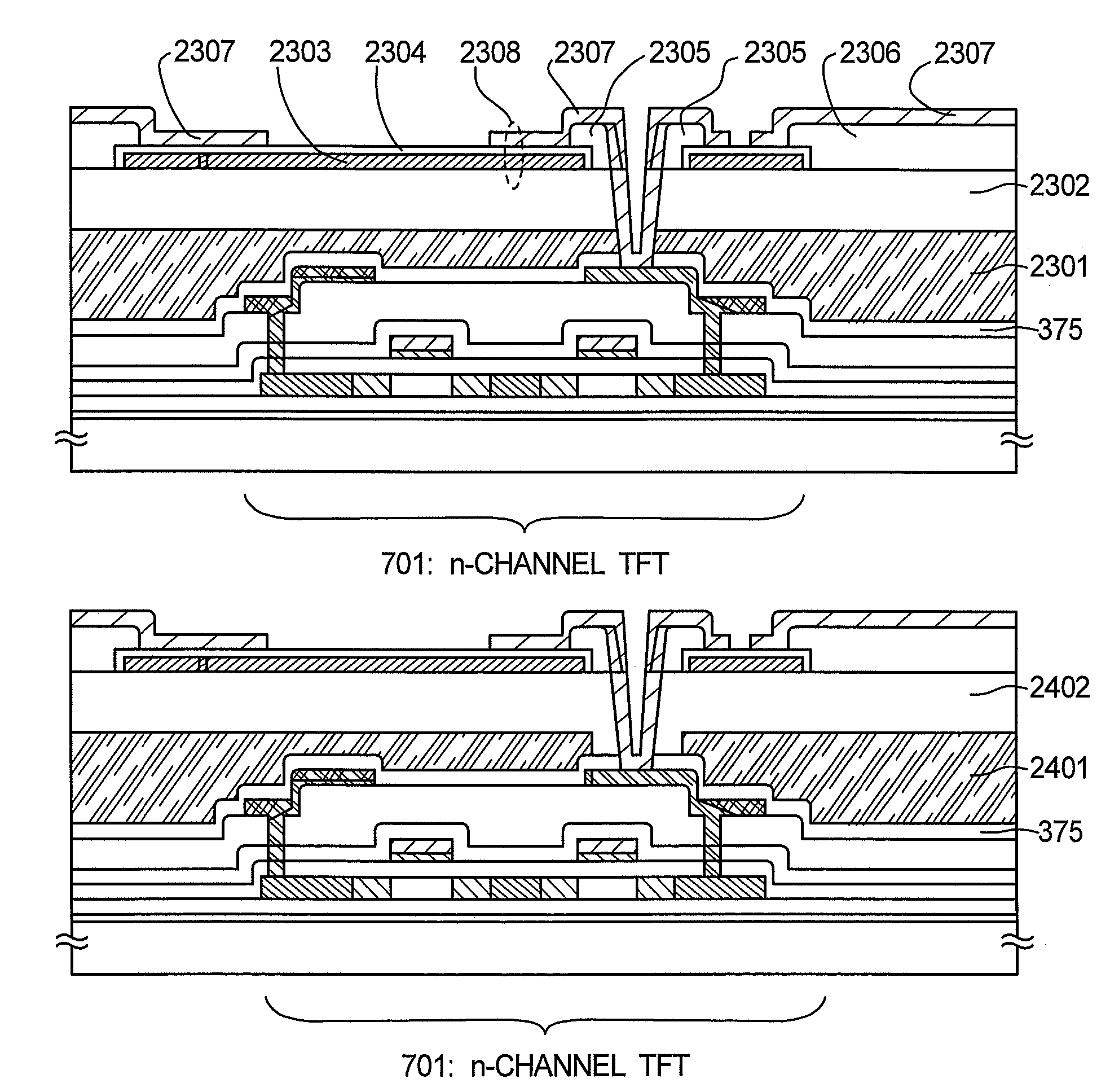
[0175]Another structure f or a storage capacitor connected to an n-channel TFT of a pixel matrix circuit on an active matrix substrate is explained in embodiment 3 using FIG. 7. Note that the same manufacturing process as in embodiment 1 is followed, through the formation of the anodic oxide film 378, for the cross sectional structure of FIG. 7, and that structures up to that point have already been explained in FIGS. 3A to 5C. In embodiment 3, therefore, only the points that differ from embodiment 1 will be focused upon and explained.

[0176]After forming the shielding film 377, and the anodic oxide film 378 obtained by anodic oxidation of the shielding film 377, in accordance with the processes of embodiment 1, spacers 702 to 704 are formed from an organic resin film. A film chosen from among polyimide, polyamide, polyimide amide, acrylic, and BCB (benzocyclobutane) can be used as the organic resin film. The spacer 702, the second interlayer insulating film 376, and the passivation ...


PUM

PropertyMeasurementUnit
temperatureaaaaaaaaaa
thicknessaaaaaaaaaa
current densityaaaaaaaaaa

Abstract

An object of the present invention is to provide a semiconductor device having high operation characteristic and reliability.The measures taken are: A pixel capacitor is formed between an electrode comprising anodic capable material over an organic resin film, an anodic oxide film of the electrode and a pixel electrode above. Since the anodic oxide film is anodically oxidized by applied voltage per unit time at 15 V / min, there is no wrap around on the electrode, and film peeling can be prevented.

Description

BACKGROUND OF THE INVENTION[0001]1. Field of the Invention[0002]The present invention relates to a semiconductor device having a circuit structured by a thin film transistor (hereafter referred to as TFT), and to a method of manufacturing the same. For example, the present invention relates to an electro-optical device, typically a liquid crystal display panel, and to electronic equipment with an electro-optical device installed as a component.[0003]Note that, throughout this specification, the semiconductor device indicates general devices that can function by using semiconductor characteristics, and that electro-optical devices, semiconductor circuits, and electronic equipment are all categorized as semiconductor devices.[0004]2. Description of the Related Art[0005]Techniques for using semiconductor thin films (with a thickness on the order of several nm to several hundreds of nm) formed on a substrate having an insulating surface to structure a thin film transistor (TFT) have bee...

Claims


Application Information

Patent Timeline
Patent Type & Authority Patents(United States)
IPC IPC(8): H01L29/04G02F1/1362H01L21/336H01L21/77H01L21/84H01L27/12H01L29/786H05B44/00
CPCG02F1/13454G02F1/136213H01L29/66757H01L29/78645H01L29/78675H01L29/786H01L27/1255H01L27/1259H01L27/1244H01L29/458H01L27/15H01L31/02164
Inventor MURAKAMI, SATOSHIYAMAZAKI, SHUNPEIKOYAMA, JUNOSAME, MITSUAKITANAKA, YUKIOHIRAKATA, YOSHIHARU
Owner SEMICON ENERGY LAB CO LTD
Why Eureka
Try Eureka