Plasma processing apparatus

a processing apparatus and plasma technology, applied in the field of magnet mechanism, can solve the problems of numerous defects in the production of semiconductor devices and unstable processing, and achieve the effect of removing processing instability

Active Publication Date: 2010-11-25
CANON ANELVA CORP
View PDF10 Cites 31 Cited by
  • Summary
  • Abstract
  • Description
  • Claims
  • Application Information

AI Technical Summary

Benefits of technology

[0013]A plasma processing apparatus mounting a magnet mechanism according to the present invention forms a magnetic field necessary for sputtering film deposition up to the most outside periphery of the target electrode and also does not form a magnetic field in a gap between the target electrode and a shield. As a result, it becomes possible to realize both of “obtaining uniform film thickness within a wafer surface by generating a necessary plasma density up to the most outside periphery of the target electrode” and “eliminating processing instability caused by a charge concentration damage of the target electrode and the shield or plasma instability, by not allowing high density plasma to be generated by a magnetic field in a gap between the target electrode and the shield”.

Problems solved by technology

If a non-uniform processing speed occurs on the wafer surface, the semiconductor device is produced as having numerous defects.
In the conventional plasma processing apparatus, however, there has been a problem that the shield 3, the target electrode 2 (first electrode), or the insulating member 4 is damaged and thereby an unstable processing is caused.

Method used


Image

  • Plasma processing apparatus
  • Plasma processing apparatus
  • Plasma processing apparatus

Examples


embodiment 1

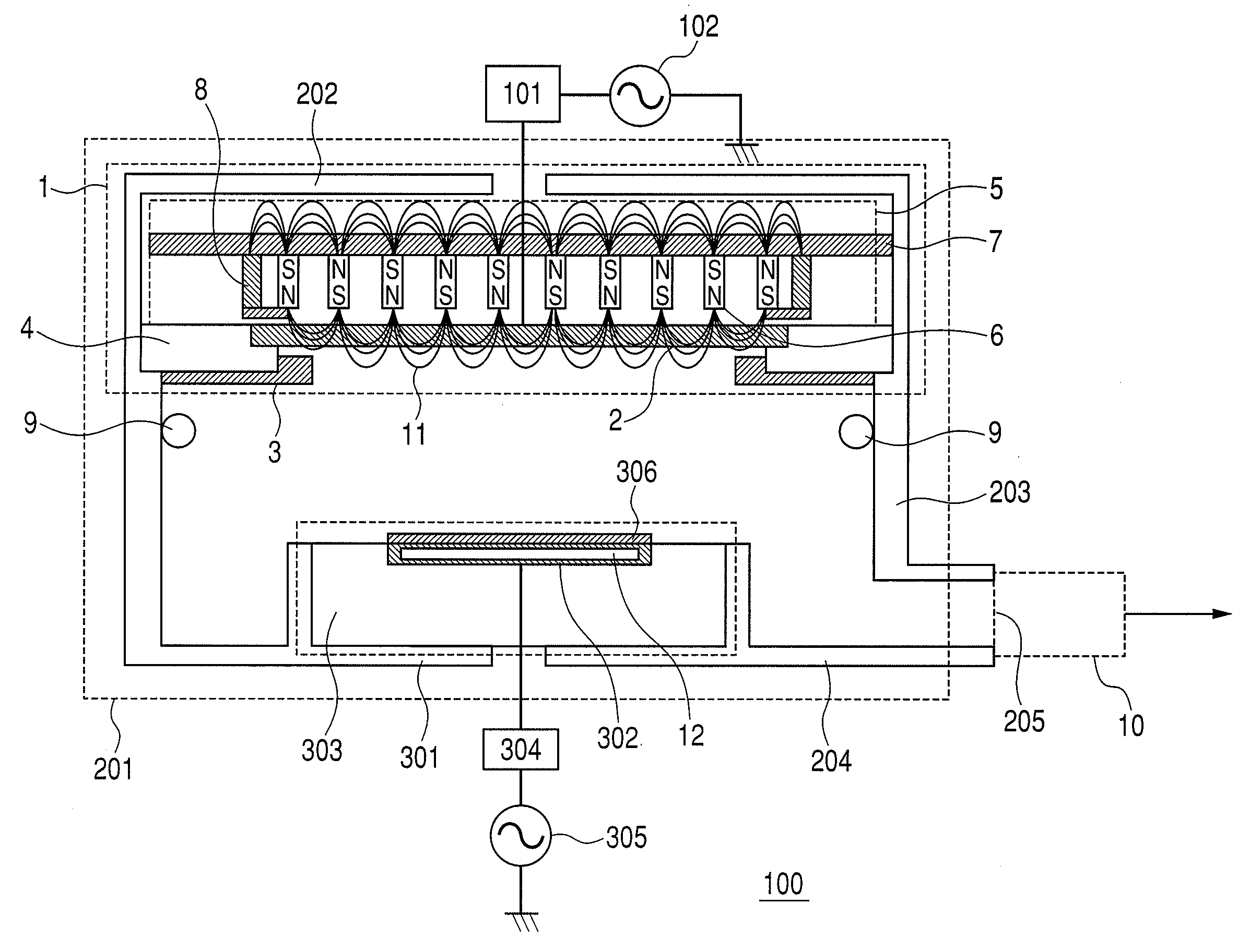
[0030]The chamber 201 disposed on the air side of the target electrode 2 (first electrode) is configured with an upper wall (ceiling wall) 202, a cylindrical side wall 203, and a bottom wall 204. A lower electrode 301 is configured with a stage holder 302 and a lower electrode insulator 303. A basic hardware structure of the plasma processing apparatus 100 of Embodiment 1 is the same as that described as the conventional technique except the part of the magnet mechanism 5. The target electrode 2 (first electrode) is disposed above the chamber 201 and insulated electrically from the chamber 201 by the upper electrode insulator 4. Main part of the target electrode 2 (first electrode) is made of a nonmagnetic metal such as Al, SUS, and Cu. A target material which is a material necessary for depositing a film on a wafer 306 is disposed on the reduced pressure side of the target electrode 2 (first electrode) corresponding to the lower surface of an upper electrode 1. The illustration of ...

second embodiment

[0044]FIG. 4 is a cross-sectional view showing a An apparatus of the present embodiment performs ionized sputtering. The ionized sputtering is a method of ionizing a sputtered particle emitted from the target electrode 2 (first electrode) and causing the sputtered particle to efficiently reach the inside of a hole by the action of the ion. By the ionized sputtering, an extremely high bottom coverage rate can be obtained compared to the collimated sputtering or the low pressure remote sputtering.

[0045]Specifically, a sputtering apparatus 400 of the present embodiment is provided with a sputtering chamber 201 having an evacuation system 10, a target electrode 2 (first electrode) provided in this sputtering chamber 201, a sputtering power source 102 for sputtering this target electrode 2 (first electrode), a gas introduction means 4 introducing predetermined gas into the sputtering chamber 201, an ionization means 600 ionizing sputtered particles emitted from the target electrode 2 (f...

third embodiment

[0050]FIG. 7 is a cross-sectional view showing a An apparatus 700 of the present embodiment is an apparatus which performs etching. As shown in FIG. 7, in a processing chamber 710 having a gas introduction pipe 708 and an exhaust port 716, a high frequency electrode 709 and a substrate mounting electrode 712 are disposed facing each other with a predetermined spacing therebetween and each of them is attached to the chamber wall via an insulator 719.

[0051]The high frequency electrode 709 includes a gas plate 702 having numerous gas blow holes 722 and a gas path 723 communicated with these gas blow holes 722, and also the high frequency electrode 711 is configured with a heat exchanger 718 having a coolant path 717 for gas plate cooling and these are connected to a first high frequency power source 709. The gas plate 702 is controlled to have a predetermined temperature by coolant supplied to the coolant path 717. On the rear side of the high frequency electrode 709 is disposed a pla...


PUM

PropertyMeasurementUnit
frequencyaaaaaaaaaa
frequencyaaaaaaaaaa
distanceaaaaaaaaaa

Abstract

A plasma apparatus includes: a chamber which can be evacuated into vacuum; first electrode disposed within the chamber; a magnet mechanism having a magnet provided apart from and above the first electrode; a second electrode provided facing the first electrode; and a magnetic shield member provided in at least one of gaps between the first electrode and the magnet mechanism and between the first electrode and the second electrode.

Description

CROSS-REFERENCES TO RELATED APPLICATIONS[0001]This application is a continuation application of International Application No. PCT / JP2007 / 074287, filed on Dec. 18, 2007, the entire contents of which are incorporated by reference herein.TECHNICAL FIELD[0002]The present invention relates to a magnet mechanism forming a magnetic field for generating plasma. The magnet mechanism is used in a plasma processing apparatus producing a semiconductor device on a silicone substrate or another substrate.BACKGROUND ART[0003]Plasma-assisted wafer processing is a process established sufficiently in the production of a semiconductor device which is usually called an integrated circuit. Conventionally, there are numerous different plasma-assisted processes such as etching, sputtering deposition, and chemical phase deposition. All of these processes must be performed so as to realize a uniform etching speed or a uniform processing speed on a wafer surface. If a non-uniform processing speed occurs on t...

Claims


Application Information

Patent Timeline
Patent Type & Authority Applications(United States)
IPC IPC(8): C23C14/34
CPCH01J37/32091H01J37/34H01J37/3266
Inventor IKEDA, MASAYOSHITANAKA, YOHIROISHI, TSUTOMU
Owner CANON ANELVA CORP
Why Eureka
Try Eureka