Method for manufacturing SOI wafer

Active Publication Date: 2008-12-04
SHIN ETSU CHEM CO LTD
View PDF8 Cites 31 Cited by
  • Summary
  • Abstract
  • Description
  • Claims
  • Application Information

AI Technical Summary

Benefits of technology

[0027]According to the method for manufacturing an SOI wafer of the present invention, etching can be performed at a relatively high etching rate on the rough etching stage, and film thickness uniformity of the SOI layer can be increased on the precise etching stage. As a result, since a

Problems solved by technology

However, this method has several problems.
In general, accurately and uniformly polishing a surface to obtain a target thickness is difficult in a polishing process called CMP (chemical mechanical polishing).
That is because constantly keeping conditions of a radial balance of various factors (e.g., a pressure or a supply amount of a slurry) concerning polishing or a polishing pad in a fixed state is difficult.
Adding the heat treatment results in occurrence of a problem of, e.g., management of contamination due to a high-temperature process, an increase in cost, or a reduction in productivity.
Further, in case of a substrate other than that formed of single-crystal silicon, e.g., a quartz substrate, a glass-transition temperature is near 1050° C.

Method used


Image

  • Method for manufacturing SOI wafer
  • Method for manufacturing SOI wafer
  • Method for manufacturing SOI wafer

Examples


Example

Example 1

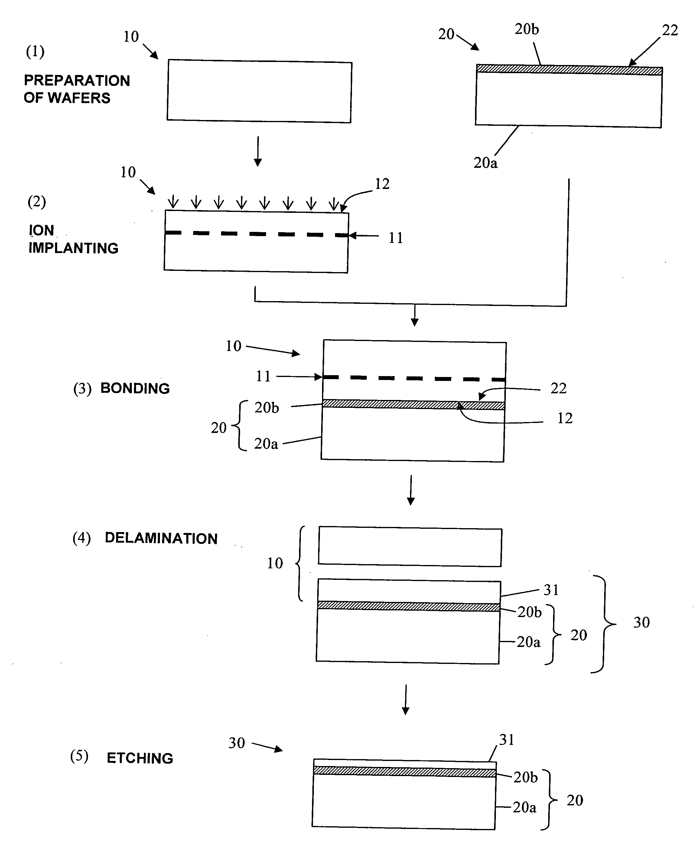
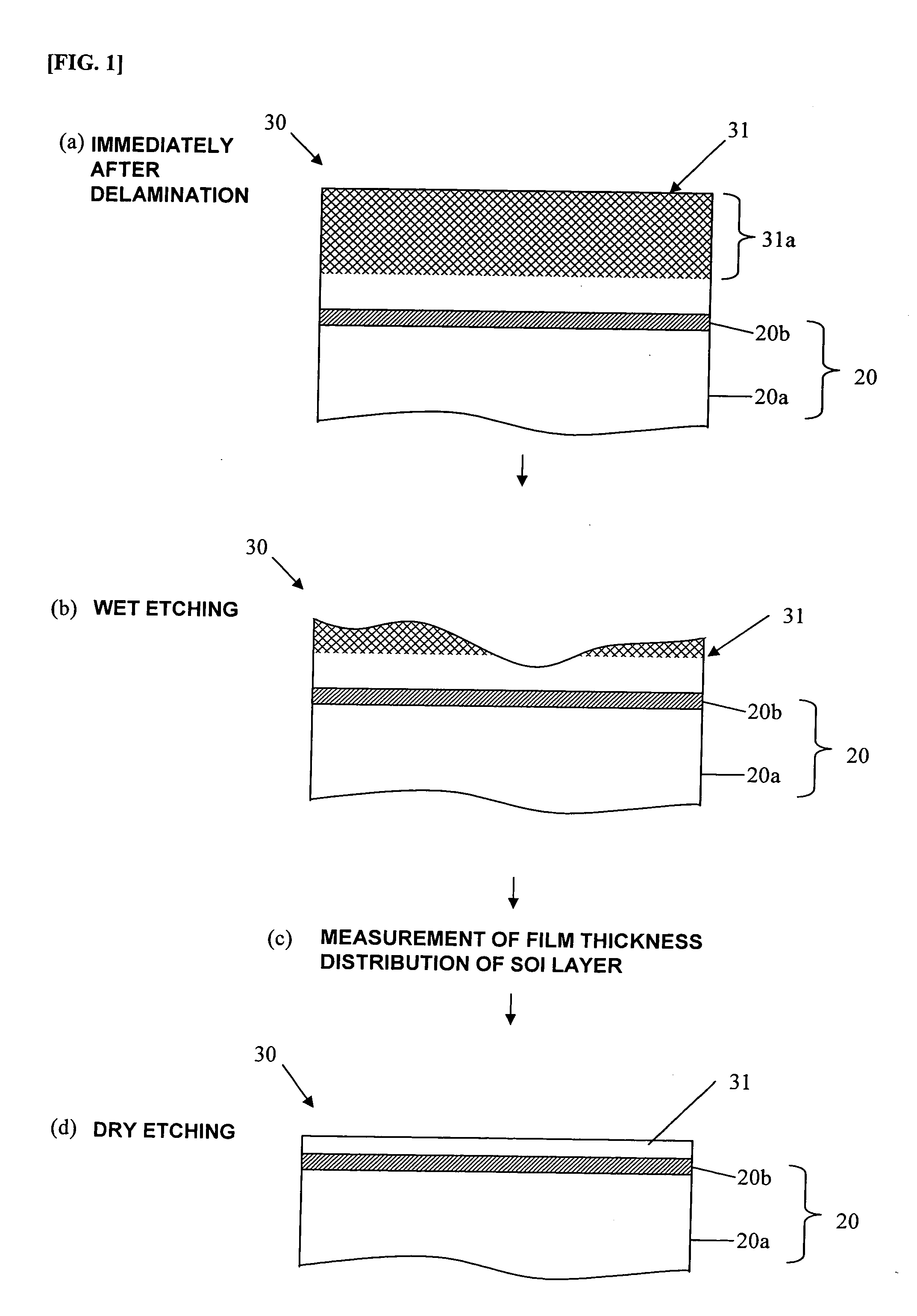
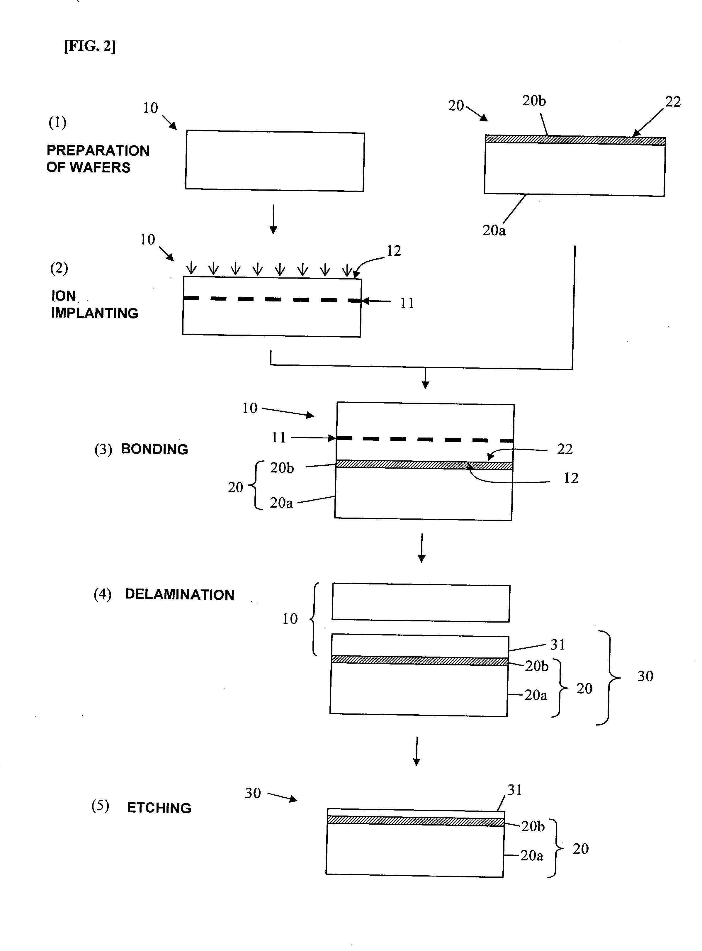
[0091]An SOI wafer was manufactured by a method of performing delamination of a donor wafer based on a heat treatment as follows in accordance with the method for manufacturing an SOI wafer of the present invention depicted in FIGS. 2 and 1.

[0092]First, as Step 1, a mirror-polished single-crystal silicon wafer having a diameter of 200 nm was prepared as a donor wafer 10. Further, a silicon oxide film layer having a thickness of 100 nm was formed on a surface of the donor wafer by thermal oxidation.

[0093]Furthermore, a single-crystal silicon wafer having a diameter of 200 mm was prepared as a handle wafer 20. Moreover, a silicon oxide film 20b having a thickness of 1 μm was formed on a surface of the handle wafer by thermal oxidation.

[0094]Then, a hydrogen ion was implanted into the donor wafer 10 through the silicon oxide film layer formed thereon, thereby forming a micro bubble layer (an ion implanted layer) 11 at an average progress depth of the ion in parallel with the s...

Example

Example 2

[0103]Like Example 1, a delamination step as Step 4 was carried out in the form of delamination based on a heat treatment, but a dry etching step as Stage c in an etching step as Step 5 was performed by using a GCIB method, thereby manufacturing an SOI wafer.

Example

Example 3

[0104]Processing was performed like Example 1, but delamination of a donor wafer 10 was carried out by applying a mechanical external force as follows.

[0105]After ion implantation at Step 2, an ion implanted donor wafer 10 was put in a plasma treatment device, nitrogen was introduced as a plasma gas, and then a high frequency of 13.56 MHz was applied to a space between parallel plate electrodes each having a diameter of 300 mm under conditions of a reduced pressure of 2 Torr (270 Pa) and a high-frequency power of 50 W, thereby effecting a high-frequency plasma treatment to an ion implanted surface for 10 seconds. In this manner, the ion implanted surface of the donor wafer 10 was subjected to a surface activation treatment.

[0106]On the other hand, a handle wafer 20 was put in a plasma treatment device, a nitrogen gas as a plasma gas was introduced into a space between narrow electrodes, and then a high frequency was applied to the space between the electrodes to generate a ...


PUM


Abstract

There is disclosed a method for manufacturing an SOI wafer comprising: a step of implanting at least one of a hydrogen ion and a rare gas ion into a donor wafer to form an ion implanted layer; a step of bonding an ion implanted surface of the donor wafer to a handle wafer; a step of delaminating the donor wafer at the ion implanted layer to reduce a film thickness of the donor wafer, thereby providing an SOI layer; and a step of etching the SOI layer to reduce a thickness of the SOI layer, wherein the etching step includes: a stage of performing rough etching as wet etching; a stage of measuring a film thickness distribution of the SOI layer after the rough etching; and a stage of performing precise etching as dry etching based on the measured film thickness distribution of the SOI layer. There can be provided A method for manufacturing an SOI wafer having high film thickness uniformity of an SOI layer with excellent productivity.

Description

BACKGROUND OF THE INVENTION[0001]1. Field of the Invention[0002]The present invention relates to a method for manufacturing an SOI wafer, and more particularly to a method for manufacturing an SOI wafer for bonding two wafers to form a thin-film SOI layer by delamination and then further reducing a film thickness of the SOI layer.[0003]2. Description of the Related Art[0004]To reduce a parasitic capacitance and increase performances of a semiconductor device, a silicon-on-insulator (SOI) wafer having a single-crystal silicon layer formed on an insulator has been widely utilized. In recent years, a demand for a thin-film SOI having an SOI layer (a single-crystal silicon layer on an insulator) of 100 nm or below has been increased to fabricate a complete depletion layer type SOI device. That is because an increase in speed of the device by reducing a film thickness of the SOI layer can be expected.[0005]As one of typical methods for fabricating an SOI wafer, there is an ion implantati...

Claims


Application Information

Patent Timeline
IPC IPC(8): H01L21/86
CPCH01L21/3065H01L21/76254H01L2924/014H01L22/20H01L22/12H01L21/20
Inventor AKIYAMA, SHOJIKUBOTA, YOSHIHIROITO, ATSUOTANAKA, KOICHIKAWAI, MAKOTOTOBISAKA, YUUJI
Owner SHIN ETSU CHEM CO LTD
Why Eureka
Try Eureka