
High-precision chip welding method of LED full-automatic die bonder

A technology of chip welding and crystal bonding machine, which is applied in the direction of electrical components, circuits, semiconductor devices, etc., can solve the problems that the crystal bonding bracket affects the accuracy of the crystal bonding work, and affects the crystal bonding work, so as to improve the loading process, facilitate the reinforcement work, The effect of not being easily polluted by static electricity

Active Publication Date: 2020-07-03
SUZHOU SUPERLIGHT MICROELECTRONICS
View PDF5 Cites 0 Cited by
  • Summary
  • Abstract
  • Description
  • Claims
  • Application Information

AI Technical Summary

Problems solved by technology

[0004] Before using the crystal bonder for crystal bonding work, it is usually necessary for technicians to prepare in advance, including melting the adhesive and fitting the crystal bonding bracket equipment to the bracket fixture and installing the bracket fixture to the designated position of the crystal bonder. Fixed, waiting for the follow-up die-bonding work, once there is an error in the manual assembly of the die-bonding bracket, it will easily affect the accuracy of the subsequent die-bonding work and affect the normal die-bonding work

Method used

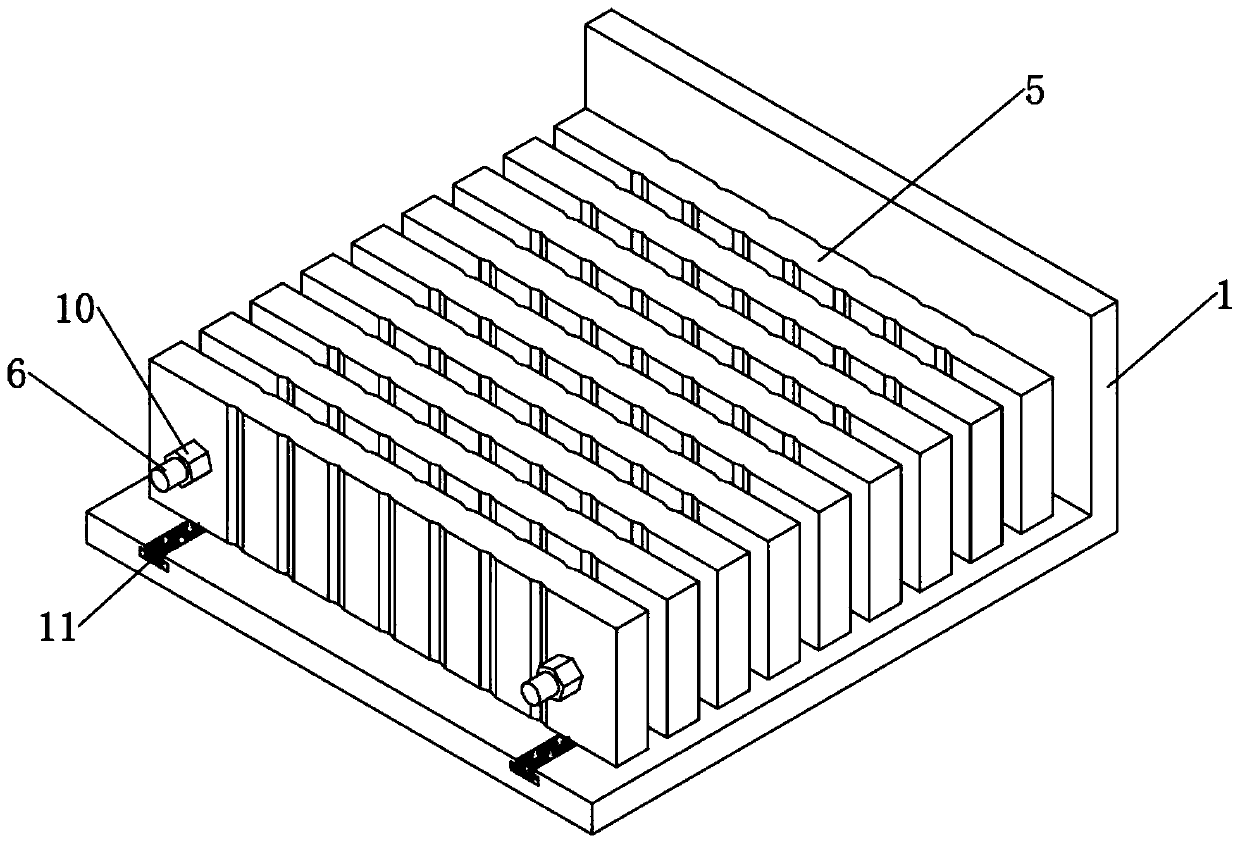
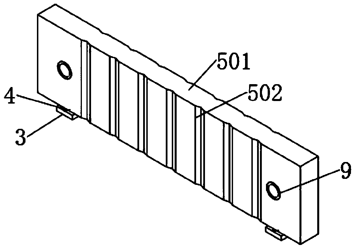
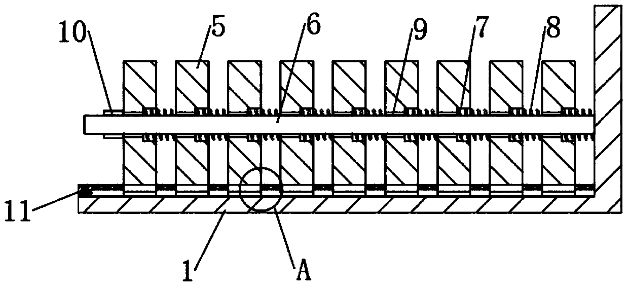

Image

  • High-precision chip welding method of LED full-automatic die bonder
  • High-precision chip welding method of LED full-automatic die bonder
  • High-precision chip welding method of LED full-automatic die bonder

Examples


Embodiment Construction

[0030] The present invention will be further described in detail below in conjunction with the accompanying drawings and specific embodiments.

[0031] A high-precision chip welding method of a fully automatic LED die-bonding machine of the present invention, the main steps include:

[0032] S1. Adhesive preparation, take out the adhesive stored in the refrigerator, keep it in a sealed state at room temperature, and let the adhesive melt slowly. After melting for 20-30 minutes, the adhesive will change from solid to liquid. Open the package of the adhesive, and use a glass rod to stir the adhesive to make the adhesive more uniform and less likely to form sediment. Finally, load the adhesive to the designated position of the die bonder. In particular, use a glass rod to stir the adhesive When adding the agent, it must be stirred slowly, so that the adhesive is not easy to become viscous under the work of the glass rod, and the stirring effect is increased;

[0033] S2. Load th...


PUM


Abstract

The invention relates to a high-precision chip welding method of an LED full-automatic die bonder. By improving the die bonding support and the support clamp, the loading process of the die bonding support is greatly improved. Rapid loading by workers is facilitated; meanwhile, a worker can conveniently take out the die bonding support from the support clamp; the support clamp can rapidly completefixation removal through the arrangement of the compression spring. A worker can conveniently take out the die bonding support from the support clamp; the T-shaped sliding groove can be effectively protected through the dustproof belt arranged at the groove opening of the T-shaped sliding groove; the influence of external impurities in the T-shaped sliding groove is not easy to occur; normal sliding of the sliding block and the connecting column is not easily influenced; and finally, for the support clamp, through the design that one of the connecting base and the connecting rod is hard and the other is soft, on the premise that the relative stability of the support main rod and the support bowl cup is guaranteed, the upper portion of the support main rod and the support bowl cup can conduct small-amplitude displacement within a controllable range, and the support clamp can be conveniently matched with reinforcing work of the die bonding support.

Description

technical field [0001] The invention relates to a high-precision chip welding method of an LED full-automatic crystal-bonding machine, in particular to a high-precision chip-welding method of an LED full-automatic crystal-bonding machine. Background technique [0002] Solid crystal is also known as Die Bond or chip loading. Die-bonding is the process of bonding the chip to the designated area of ​​the bracket through colloid (for LEDs, generally conductive glue or insulating glue), forming a thermal path or an electrical path, and providing conditions for subsequent wiring connections. The main working process of the machine is dispensing glue on the bottom frame (1), dotting the crystal-bonding glue inside the cup, loading the film into the T-shaped chute (2), putting the LED chip inside the dispensing cup, and the slider ( 3) Baking, put the solid crystal lamp cup in the oven and bake three steps, and the above three steps have been greatly automated. Under the control of...

Claims


Application Information

Patent Timeline
IPC IPC(8): H01L33/48
CPCH01L33/48H01L2933/0033
Inventor 乔金彪
Owner SUZHOU SUPERLIGHT MICROELECTRONICS
Learn More