

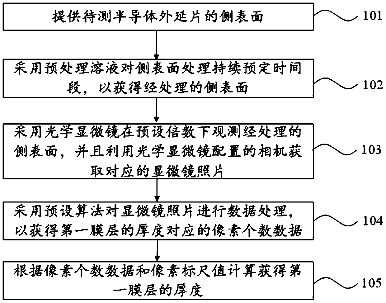
Method for measuring thickness of film in semiconductor epitaxial wafer
A technology for semiconductors and epitaxial wafers, which is applied in semiconductor/solid-state device testing/measurement, measuring devices, instruments, etc. It can solve the problems of complex process steps, difficulty in accurately knowing the depth of wet etching, and expensive steps
- Summary
- Abstract
- Description
- Claims
- Application Information
AI Technical Summary
Problems solved by technology
Method used
Image

Examples
Embodiment Construction
[0041]The following will clearly and completely describe the technical solutions in the embodiments of the present invention with reference to the accompanying drawings in the embodiments of the present invention. Obviously, the described embodiments are only some, not all, embodiments of the present invention. Based on the embodiments of the present invention, all other embodiments obtained by persons of ordinary skill in the art without creative efforts fall within the protection scope of the present invention.
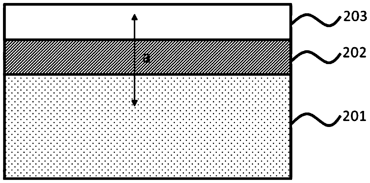
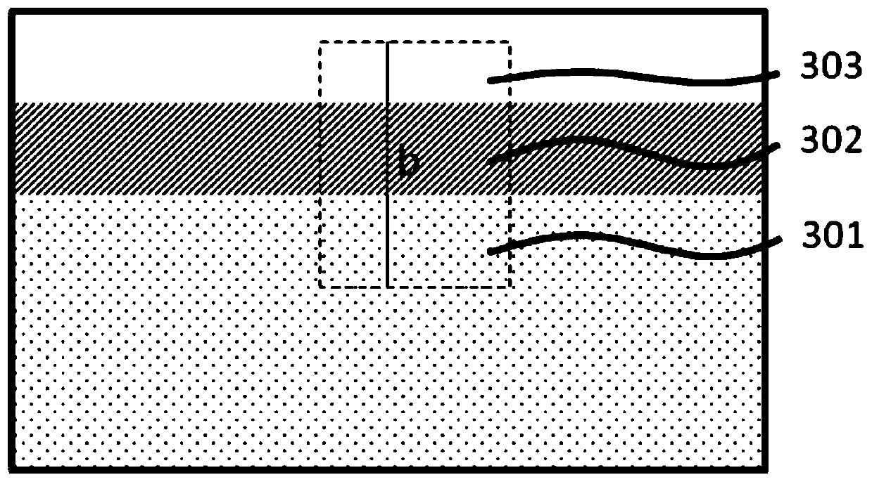
[0042] In mass production of molecular beam epitaxy, when conducting certain electrical performance tests (for example, Hall effect tests) on semiconductor epitaxial wafers containing GaAs / AlGaAs / AlAs combined epitaxial layers, at least a part of the epitaxial wafer to be tested is required The sample (eg, a small sample obtained by cleaving from an epitaxial wafer to be tested) is subjected to etching (eg, wet etching) and electrodes are prepared, thereby forming th...
PUM
| Property | Measurement | Unit |
|---|---|---|
| thickness | aaaaa | aaaaa |
| thickness | aaaaa | aaaaa |
| thickness | aaaaa | aaaaa |
Abstract
Description
Claims
Application Information