Flattening device and method for circuit board processing

A flattening device and a technology for circuit boards, which are applied in the directions of cleaning methods, separation methods, cleaning methods and utensils using gas flow, which can solve the problems of sticking dust on the surface of flexible circuit boards, uneven substrate tension, and uneven winding. problem, to achieve the effect of convenient and quick dust removal, simple steps and increased tension

Pending Publication Date: 2020-07-24
浙江新连宇电子有限公司
View PDF0 Cites 0 Cited by
  • Summary
  • Abstract
  • Description
  • Claims
  • Application Information

AI Technical Summary

Problems solved by technology

[0004] However, in the actual processing and production process, due to the uneven tension of the substrate itself, wrinkles and uneven winding often occur during the manufacturing process, and at the same time, it is easy to cause dust to stick to the surface of the flexible circuit board.

Method used


Image

  • Flattening device and method for circuit board processing
  • Flattening device and method for circuit board processing
  • Flattening device and method for circuit board processing

Examples


Embodiment Construction

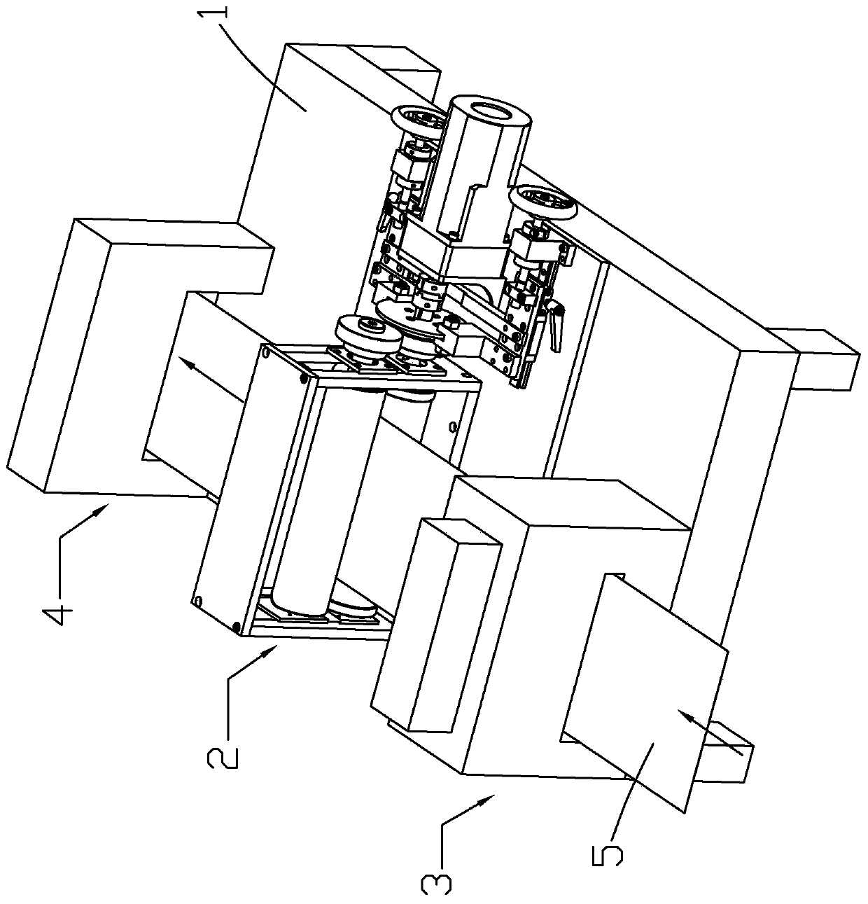
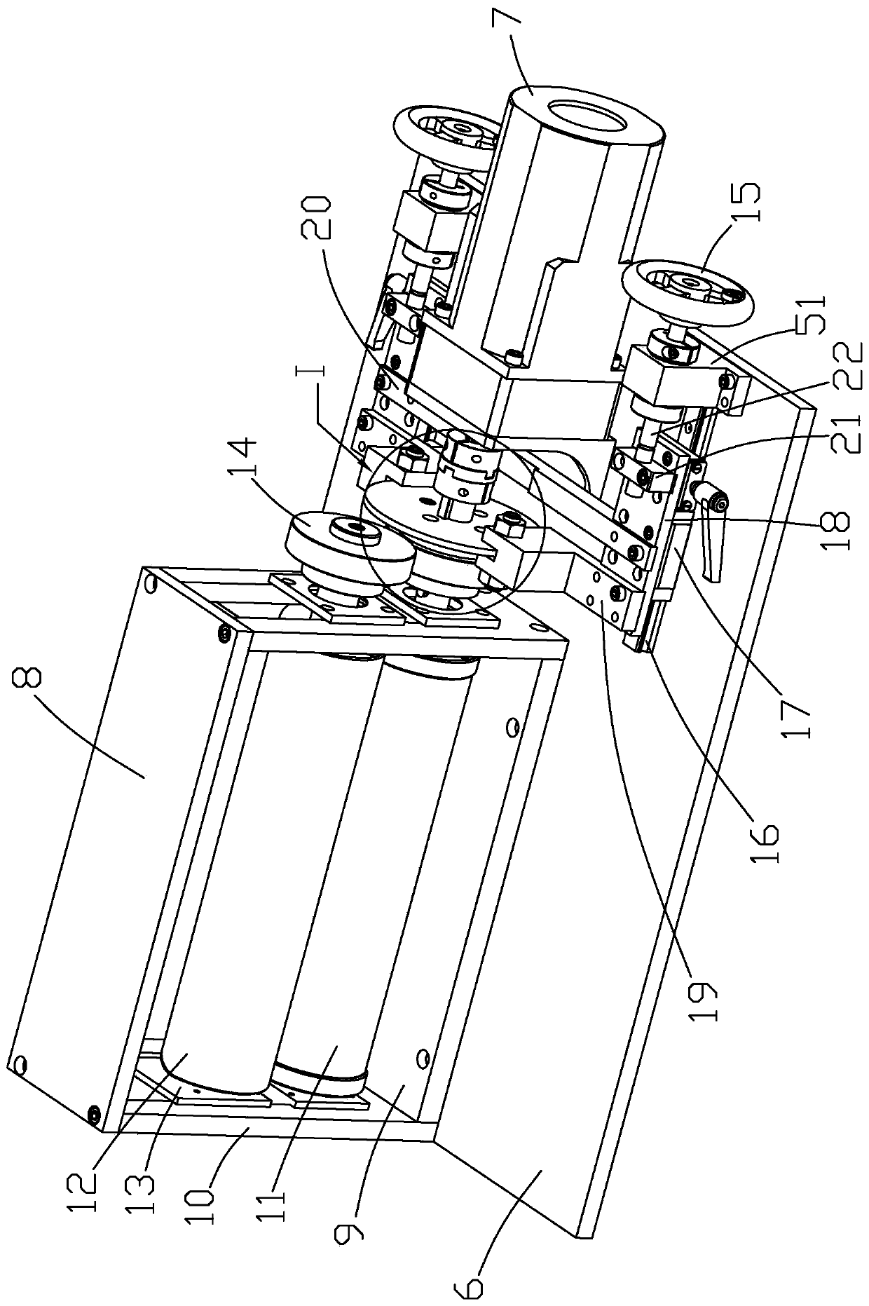
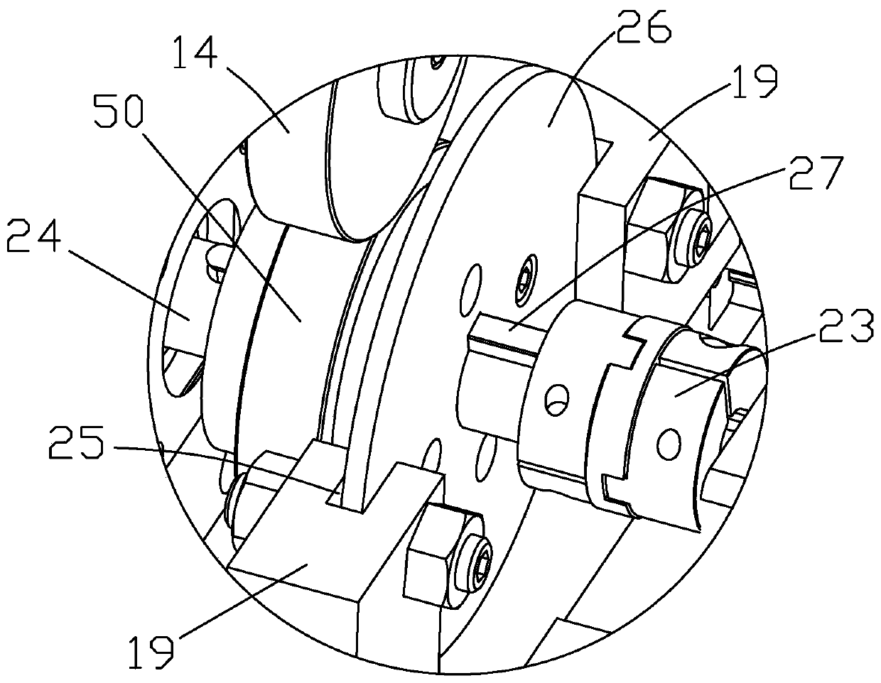
[0060] Such as Figure 1 to Figure 6 As shown, it is a flattening device for circuit board processing in the present invention, including a flattening platform 1, a flattening mechanism 2, a dust suction mechanism 3 and a detection mechanism 4, and the flattening mechanism 2, the dust suction mechanism 3 and the detection mechanism 4 are all located at On the top surface of the unfolding platform 1, the dust suction mechanism 3 and the detection mechanism 4 are located on both sides of the flattening mechanism 2, and the circuit board 5 passes through the dust suction mechanism 3, the flattening mechanism 2 and the detection mechanism 4 in sequence; The design can remove dust from the circuit board 5 that needs to be flattened to prevent dust from adhering to the surface of the circuit board 5 during the flattening process, which will affect the quality and service life of the circuit board 5. The flattening mechanism 2 can The flexible circuit board 5 is flattened to prevent ...


PUM


Abstract

The invention discloses a flattening device and method for circuit board processing. The flattening device comprises a flattening platform, a flattening mechanism, a dust absorption mechanism and a detection mechanism. The flattening mechanism, the dust absorption mechanism and the detection mechanism are all located on the top surface of the flattening platform, and the dust absorption mechanismand the detection mechanism are located on two sides of the flattening mechanism. A circuit board penetrates through the dust absorption mechanism, the flattening mechanism and the detection mechanismin sequence. The method includes the steps of flattening platform processing, dust absorption mechanism installation, flattening mechanism installation, detection mechanism installation and circuit board flattening detection. According to the flattening device and method for circuit board processing, the circuit board that needs to be flattened can be dedusted, dust is prevented from sticking tothe surface of the circuit board during the flattening process, the circuit board is prevented from wrinkling and unwinding inequality in the manufacturing process, and the processing quality of the circuit board is improved. The flattening detection method of the circuit board is simple in steps, the automatic dust absorption, flattening and scanning of the circuit board can be realized, the phenomenon of wrinkling and unwinding inequality in the manufacturing process can be prevented, and the processing quality of the circuit board is improved.

Description

technical field [0001] The invention relates to a flattening device and method for circuit board processing. Background technique [0002] Flexible circuit board is a highly reliable and excellent flexible printed circuit board made of polyimide or polyester film, referred to as soft board or FPC, with high wiring density and light weight. , Thin thickness, good bending properties. [0003] The flexible circuit board embeds the circuit design on the bendable thin and light plastic sheet, so that a large number of precision components can be stacked in a narrow and limited space, thereby forming a bendable flexible circuit. This kind of circuit can be bent and folded at will, light in weight, small in size, good in heat dissipation, and easy to install. [0004] However, in the actual processing and production process, due to the uneven tension of the substrate itself, wrinkles and uneven winding often occur during the manufacturing process, and it is easy to cause dust to ...

Claims


Application Information

Patent Timeline
Patent Type & Authority Applications(China)
IPC IPC(8): B29C53/18B29C53/80B08B5/04B29C37/00B01D46/12B29L31/34
CPCB01D46/12B08B5/043B29C37/00B29C53/18B29C53/80B29C2037/90B29L2031/3425
Inventor 汪海涛周利军詹旭刘建军
Owner 浙江新连宇电子有限公司
Why Eureka
Try Eureka