Supercharge Your Innovation With Domain-Expert AI Agents!

Wide linear array image sensor

A technology of image sensor and image sensor chip, which is applied in image communication, electric solid-state devices, semiconductor devices, etc., to achieve the effect of eliminating pixel overlap and line difference, eliminating pixel overlap, and improving image quality

Pending Publication Date: 2020-07-28
深圳市光太科技有限公司
View PDF0 Cites 0 Cited by
  • Summary
  • Abstract
  • Description
  • Claims
  • Application Information

AI Technical Summary

Problems solved by technology

[0003] The purpose of the present invention is to provide a wide-width linear array image sensor, which solves the problem that the existing splicing method requires software splicing and compensation

Method used


Image

  • Wide linear array image sensor
  • Wide linear array image sensor

Examples


Embodiment

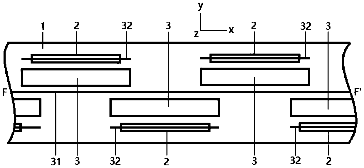
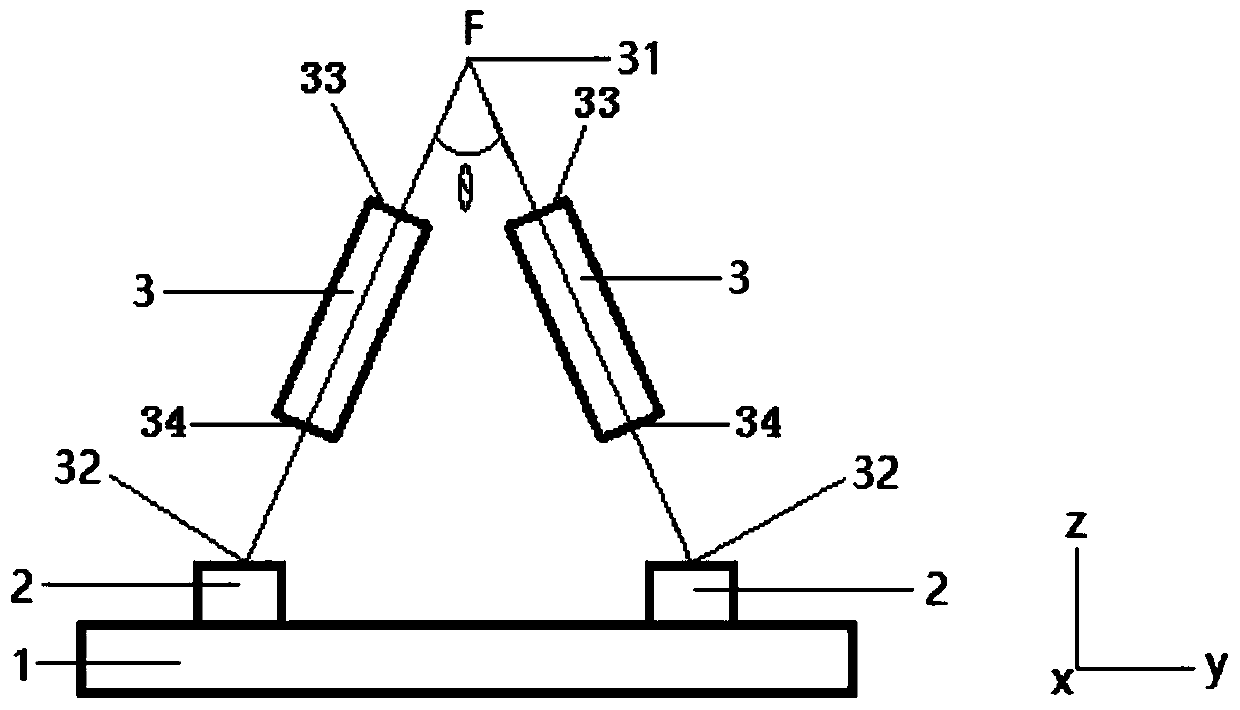
[0021] This embodiment provides a wide-width line array image sensor, such as figure 1 As shown, it includes a circuit board 1, a plurality of linear image sensor chips 2 and a plurality of self-focusing lens arrays 3, and the self-focusing lens array 3 is above the circuit board 1 along the length direction (x direction) of the circuit board 1 ) are arranged in a staggered manner, the object end 33 of the self-focus lens array 3 faces upward, the image end 34 of the self-focus lens array 3 faces downward, and the optical axes of the object end 33 of the two adjacent self-focus lens arrays 3 form an angle of θ, 10°≤θ≤90°, such as figure 2 shown. figure 1 and figure 2 F-F' in represents object line 31, establishes three-dimensional coordinate system with circuit board 1 as xy plane, x represents the x-axis of three-dimensional coordinate system, y represents the y-axis of three-dimensional coordinate system, and z represents the z-axis of three-dimensional coordinate system...


PUM


Abstract

The invention relates to a wide linear array image sensor. The wide linear array image sensor comprises a circuit board, linear array image sensing chips and self-focusing lens arrays, wherein a plurality of the self-focusing lens arrays are arranged above the circuit board in a staggered mode in a length direction, the object ends of every two adjacent self-focusing lens arrays face upwards, theimage ends of every two adjacent self-focusing lens arrays face downwards, and the object lines of every two adjacent self-focusing lens arrays are located on the same straight line and are continuous; the linear array image sensing chips corresponding to the self-focusing lens arrays are mounted on the circuit board; and the image lines of the self-focusing lens arrays are allowed to completely cover the photosensitive center lines of the linear array image sensing chips corresponding to the self-focusing lens arrays, and the object lines corresponding to the image lines covering the two adjacent linear array image sensing chips are continuous and are not overlapped. An image acquired by the wide linear array image sensor is free of the problems of pixel overlapping and line difference, so the image does not need to be spliced and compensated by software, and the manufacturing cost and the maintenance cost of the wide linear array image sensor are reduced.

Description

technical field [0001] The invention relates to the field of linear array image sensors, in particular to a wide-width linear array image sensor manufactured by splicing. Background technique [0002] The linear array image sensor is mainly composed of a linear array image sensor chip and a lens. The scanning range of a traditional linear array image sensor is generally smaller than the A3 format. The sensor chips can be seamlessly connected, but the self-focusing lens array is difficult to seamlessly connect. The entire self-focusing lens array with a width larger than A3 is expensive, so the wide-format line array image sensors all adopt a staggered splicing method to reduce costs. The traditional splicing method has problems such as partial pixel overlap and line difference in the stepping direction, which need to be spliced ​​and compensated by software. Every repair and replacement needs to be re-adjusted, and the maintenance cost is high. Therefore, existing stitching...

Claims


Application Information

Patent Timeline
IPC IPC(8): H01L27/146H04N5/369
CPCH01L27/14634H01L27/14627H04N25/70
Inventor 李宏明肖昌林刘成名肖建全
Owner 深圳市光太科技有限公司
Features
  • R&D
  • Intellectual Property
  • Life Sciences
  • Materials
  • Tech Scout
  • Unparalleled Data Quality
  • Higher Quality Content
  • 60% Fewer Hallucinations
Learn More