
Active matrix type flat-panel display device

a flat-panel display and active matrix technology, applied in the field of active matrix type flat-panel display devices, can solve the problems of rising edges, delay by a certain period t, and the picture quality of the display device to deteriorate, so as to achieve the effect of greatly improving the picture quality

Inactive Publication Date: 2005-12-06
SEMICON ENERGY LAB CO LTD +1
View PDF53 Cites 12 Cited by
  • Summary
  • Abstract
  • Description
  • Claims
  • Application Information

AI Technical Summary

Benefits of technology

[0006]It is therefore an object of the present invention to provide an active matrix type flat-panel display device whereby picture quality can be greatly improved by preventing overlap between selection signals of neighboring columns or lines from occurring.
[0007]According to the present invention, an active matrix type flat-panel display device includes a flat substrate, a plurality of light emissive elements arranged two dimensionally along columns and lines on the flat substrate, a plurality of selection switches formed on the flat substrate, for sequentially selecting the light emissive elements to provide video signals thereto, selection signal generation circuits for providing selection signals which drive the selection switches in sequence so as to two dimensionally scan the light emissive elements, and a selection signal control circuit for preventing the selection signals to be outputted from the selection signal generation circuits for a predetermined period of time so as to eliminate overlap between the selection signals.
[0008]Thus, overlap between selection signals of neighboring columns or lines can be prevented from occurring causing picture quality to be greatly improved.

Problems solved by technology

These high power TFTs for the column-selecting transistors result in a time constant, determined by their large gate capacitance and on-resistance of circuits connected to the gates of the column-selecting transistors, to extremely increase and thus cause rise edges and fall edges of selection signals, applied to these respective gates, to delay by a certain period ΔT.
As a result, a video signal for light emissive element positioned at a certain column and a certain line will stray into a next light element positioned at the neighboring column and the same line causing picture quality of the display device to deteriorate.

Method used


Image

  • Active matrix type flat-panel display device
  • Active matrix type flat-panel display device
  • Active matrix type flat-panel display device

Examples


Embodiment Construction

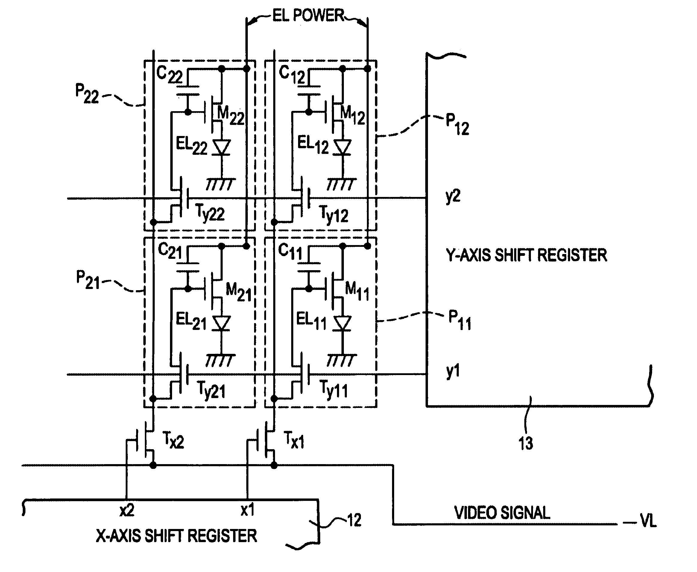
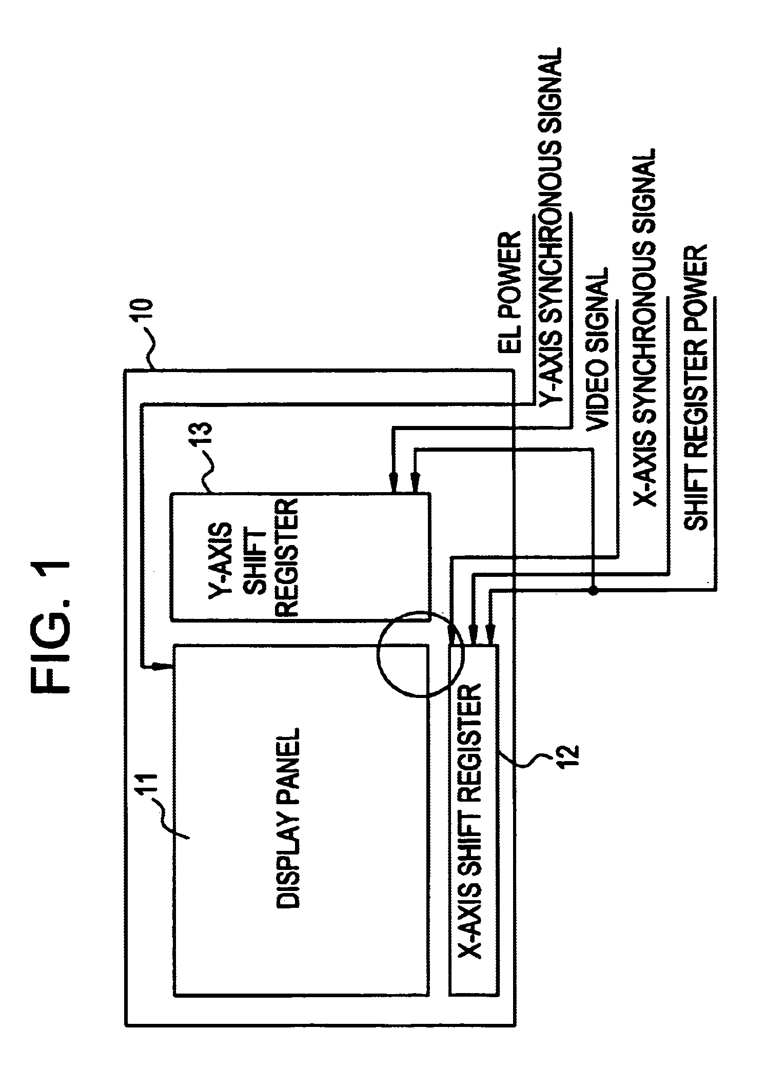
[0023]FIG. 1 schematically shows a part of a preferred embodiment of an active matrix type flat-panel display device according to the present invention.

[0024]As illustrated in the figure, the display device 10 has a flat display panel 11, an X-axis shift register 12 and a Y-axis shift register 13.

[0025]The flat display panel 11 has a substrate (not indicated) and a plurality of picture elements of light emissive elements which are two dimensionally arranged along X-axis and Y-axis in matrix on the substrate. In this embodiment, the light emissive elements are constituted by organic EL (electro luminescent) elements. To the respective picture elements of the display panel 11, EL power and video signal are supplied. To the X-axis shift register 12, shift register power and an X-axis synchronous signal are supplied. To the Y-axis shift register 13, shift register power and a Y-axis synchronous signal are supplied.

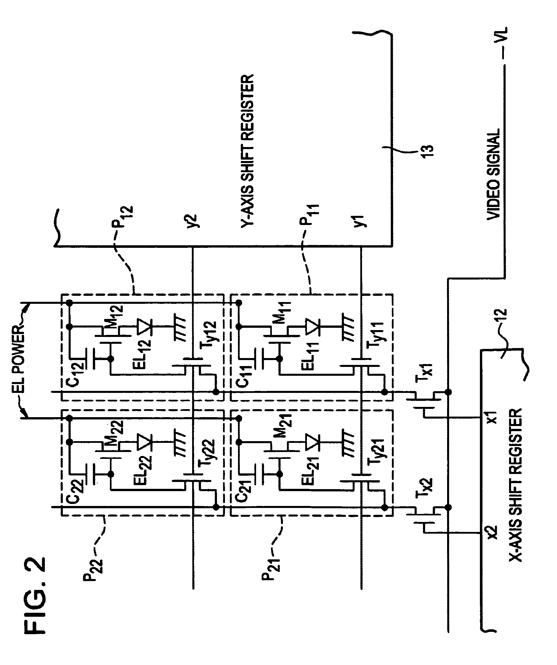
[0026]FIG. 2 is an enlarged view of a circled portion in FIG. 1. As will ...


PUM


Abstract

An active matrix type flat-panel display device includes a flat substrate, a plurality of light emissive elements arranged two dimensionally along columns and lines on the flat substrate, a plurality of selection switches formed on the flat substrate, for sequentially selecting the light emissive elements to provide video signals thereto, selection signal generation circuits for providing selection signals which drive the selection switches in sequence so as to two dimensionally scan the light emissive elements, and a selection signal control circuit for preventing the selection signals from being output from the selection signal generation circuits for a predetermined period of time so as to eliminate overlap between the selection signals.

Description

[0001]This application is a Division of application Ser. No. 08 / 547,919 filed Oct. 25, 1995 now U.S. Pat. No. 5,986,632.FIELD OF THE INVENTION[0002]The present invention relates to an active matrix type flat-panel display device with light emissive elements such as EL (electro luminescent) elements or light nonemissive elements such as liquid crystal elements arranged two dimensionally in matrix and sequentially driven by means of respective drive thin film transistors (TFTs).DESCRIPTION OF THE RELATED ART[0003]An active matrix type flat-panel display device with light emissive elements and respective driver TFTs which are two dimensionally arranged along X-axis and Y-axis in matrix is known. In such a device, the drive TFTs of the respective picture elements are sequentially scanned by column-selecting transistors (TFTs) and line-selecting transistors (TFTs). Each of the column-selecting transistors, which are sequentially turned on by means of an X-axis shift register, is connecte...

Claims


Application Information

Patent Timeline
IPC IPC(8): G09G3/20G09G3/22G09G3/30G09G3/32G09G3/36
CPCG09G3/20G09G3/3233G09G3/3291G09G3/3688G09G3/22G09G3/30G09G3/32G09G3/3208G09G3/3266G09G3/3283G09G3/3651G09G2300/0842G09G2310/0267G09G2310/0275G09G2310/0286G09G2310/08G09G2320/0209
Inventor TAKAYAMA, ICHIROARAI, MICHIO
Owner SEMICON ENERGY LAB CO LTD
Learn More