Depletion mode transistor driving circuit and chip

A technology of depletion-mode transistors and drive circuits, applied in electrical components, electronic switches, pulse technology, etc., can solve the problems of switching speed limitation and affecting the high-speed switching characteristics of depletion-type transistors, so as to avoid parasitic voltage breakdown and avoid Effects with limited application scenarios

Active Publication Date: 2022-06-28
SHENZHEN XINER SEMICON TECH CO LTD
View PDF0 Cites 0 Cited by
  • Summary
  • Abstract
  • Description
  • Claims
  • Application Information

AI Technical Summary

Problems solved by technology

[0005] An embodiment of the present invention provides a depletion-mode transistor drive circuit to solve the problem of switching speed limitation and affecting the high-speed switching characteristics of the depletion-mode transistor in the process of using a low-voltage MOS tube to drive the depletion-mode transistor

Method used


Image

  • Depletion mode transistor driving circuit and chip
  • Depletion mode transistor driving circuit and chip
  • Depletion mode transistor driving circuit and chip

Examples


Embodiment Construction

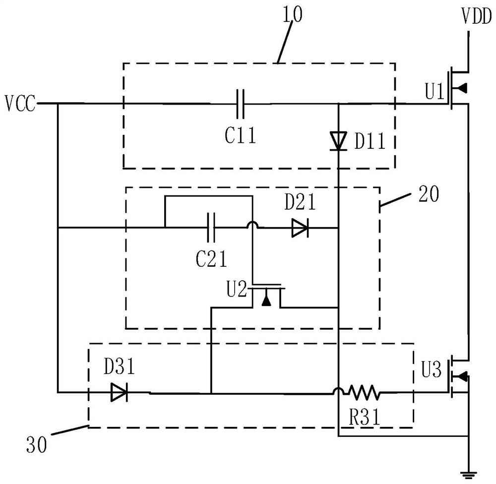
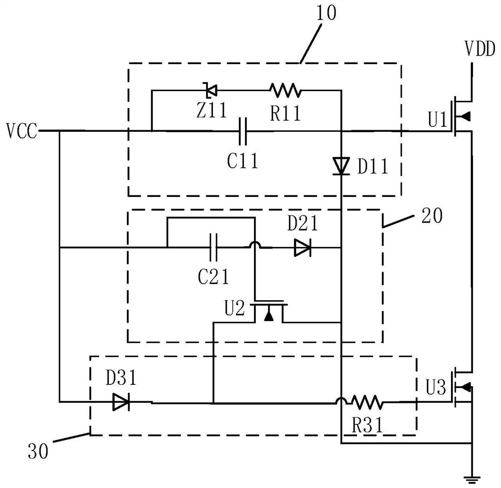
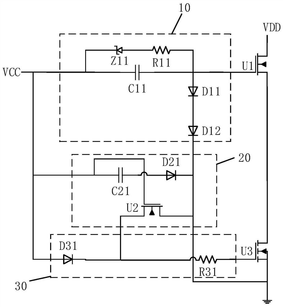
[0034] The technical solutions in the embodiments of the present invention will be clearly and completely described below with reference to the accompanying drawings in the embodiments of the present invention. Obviously, the described embodiments are part of the embodiments of the present invention, but not all of the embodiments. Based on the embodiments of the present invention, all other embodiments obtained by those of ordinary skill in the art without creative efforts shall fall within the protection scope of the present invention.

[0035] It should be understood that the present invention may be embodied in different forms and should not be construed as limited to the embodiments set forth herein. Rather, these embodiments are provided so that this disclosure will be thorough and complete, and will fully convey the scope of the invention to those skilled in the art. In the drawings, the size and relative sizes of layers and regions may be exaggerated for clarity. Like ...


PUM


Abstract

The invention discloses a depletion transistor driving circuit and a chip. In this circuit, the drain of the low-voltage MOS tube is connected to the source of the main depletion-mode transistor, and the source of the low-voltage MOS tube is grounded; the indirect locking circuit is connected to the power supply terminal and the gate of the low-voltage MOS tube to drive the low-voltage MOS tube Turn on, lock the low-voltage MOS tube in the normally-on state after the main depletion-mode transistor is turned on for the first time; the direct drive circuit is connected with the power supply terminal, the gate of the main depletion-mode transistor and the source of the low-voltage MOS tube, and is used to directly drive the main consumption Turn on or off the exhaust transistor; the auxiliary drive circuit is connected to the power supply terminal, the direct drive circuit, the indirect locking circuit and the source of the low-voltage MOS tube, and is used to drive the indirect locking circuit to lock the low-voltage MOS tube in the normally open state; under the power supply terminal After power-on, the low-voltage MOS transistor is driven to turn off, and the direct drive circuit is controlled to turn off the main depletion-mode transistor. The circuit can increase the switching speed of the low-voltage MOS tube and ensure the high-speed switching characteristics of the main depletion transistor.

Description

technical field [0001] The present invention relates to the technical field of semiconductor driving, and in particular, to a depletion transistor driving circuit and a chip. Background technique [0002] Depletion-mode transistors are an important part of power electronic devices. They are generally unipolar devices and use electrons as the medium of current transmission. Due to the fast transmission speed of electrons, they can be widely used in high frequency and high power density fields. [0003] Depletion-mode transistors are normally-on devices that generally require a negative voltage to be turned off, making their reliability low in practical applications. For example, isolated power supplies or charge pumps are widely used to create negative voltages to control depletion transistors. During operation, if the isolated power supply or charge pump fails, the depletion transistors will be turned on, endangering the product and Personal safety and high manufacturing co...

Claims


Application Information

Patent Timeline
Patent Type & Authority Patents(China)
IPC IPC(8): H03K17/687
CPCH03K17/687
Inventor 张益鸣刘杰
Owner SHENZHEN XINER SEMICON TECH CO LTD
Why Eureka
Try Eureka