tft, tft array substrate, manufacturing method thereof, display panel, display device

An array substrate and substrate technology, which is applied to display panels and display devices, TFT, TFT array substrates and their manufacturing fields, can solve the problems of large parasitic capacitance, susceptibility to damage of semiconductor active layers, increased risk of discharge breakdown, and the like, Achieve the effect of reducing parasitic capacitance and avoiding the risk of discharge breakdown

Active Publication Date: 2017-12-26
SHANGHAI TIANMA MICRO ELECTRONICS CO LTD +1
View PDF3 Cites 0 Cited by
  • Summary
  • Abstract
  • Description
  • Claims
  • Application Information

AI Technical Summary

Problems solved by technology

[0004] In the process of fabricating thin film transistors on the substrate in the prior art, since the semiconductor active layer is easily damaged, an etch barrier layer is formed above the semiconductor active layer to protect the semiconductor active layer. When the barrier layer is etched, the gate insulating layer will be over-etched at the edge of the semiconductor active layer.
As a result, the risk of discharge breakdown between the source and drain metals and the gate metal increases, and because there is only one gate insulating layer between the source and drain metals and the gate metal, there is a large parasitic capacitance

Method used


Image

  • tft, tft array substrate, manufacturing method thereof, display panel, display device
  • tft, tft array substrate, manufacturing method thereof, display panel, display device
  • tft, tft array substrate, manufacturing method thereof, display panel, display device

Examples


Embodiment 1

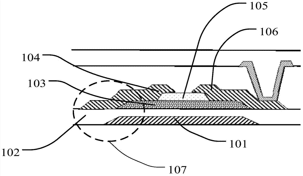
[0048] Please refer to image 3 , image 3 It is a schematic structural diagram of a thin film transistor array substrate provided in Embodiment 1 of the present invention. From image 3 It can be obtained that the thin film transistor array substrate provided in this embodiment includes: a substrate (not shown in the figure); a plurality of intersecting and insulated scanning lines (not shown in the figure) and a plurality of data lines arranged on the substrate line 204, and a plurality of pixel units defined by the scan line and the data line 204; a thin film transistor disposed in the pixel unit.

[0049] The thin film transistor comprises: a gate 201; a gate insulating layer 202 disposed on the gate 201; a mutually insulated semiconductor active layer 203 disposed on the gate insulating layer 202; disposed on the semiconductor The etch barrier layer 205 on the active layer 203; the source electrode 211 and the drain electrode 210 arranged on the semiconductor active la...

Embodiment 2

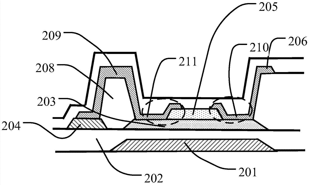
[0056] Please refer to Figure 4 to Figure 10 , Figure 4 to Figure 10 It is a schematic structural diagram of the array substrate during the manufacturing process provided by Embodiment 2 of the present invention. A method for manufacturing a thin film transistor array substrate provided in this embodiment includes: providing a substrate (not shown in the figure); forming a first metal layer on the substrate, patterning the metal layer, and forming a gate 201, such as Figure 4 As shown; a gate insulating layer 202 is formed on the gate 201; a semiconductor layer is formed on the gate insulating layer 202, and the semiconductor layer is patterned to form a semiconductor active layer 203, as Figure 5 As shown; a first insulating layer is formed on the semiconductor active layer 203, and the insulating layer is patterned to form an island-shaped etch stop layer 205, as Figure 6 As shown; a second metal layer is formed on the gate insulating layer 202, and the second metal ...


PUM


Abstract

The invention describes a TFT, a TFT array substrate and a manufacturing method thereof, a display panel and a display apparatus. The TFT comprises a gate electrode, a gate electrode insulating layer arranged on the gate electrode, a semiconductor active layer arranged on the gate electrode insulating layer, an etching barrier layer arranged on the semiconductor active layer, and a source electrode and a drain electrode both arranged on the semiconductor active layer. Both the source electrode and the drain electrode do not cover the edges of the semiconductor active layer. When formed, the source electrode and the drain electrode are not connected with the semiconductor active layer; then an insulating film is used to pave the edges of the semiconductor active layer; and then the source electrode and the drain electrode are connected to the semiconductor active layer by means of a transparent conductive layer. Therefore, the discharge breakdown risk of metal of the source electrode and the drain electrode to the gate electrode caused by over-etching of the etching resisting layer is avoided. Besides, one more insulating film between the source and the drain electrodes and gate lines reduces the parasitic capacitance.

Description

technical field [0001] The present invention relates to the display field, in particular to a TFT, a TFT array substrate and a manufacturing method thereof, a display panel and a display device including the TFT array substrate. Background technique [0002] The flat panel display is currently the mainstream display, and is widely used in electronic products such as computer screens, mobile phones, personal digital assistants, and flat-screen TVs because of its thin and light appearance, power saving, and no radiation. [0003] In the prior art, flat panel displays are divided into active matrix displays and passive matrix displays in terms of driving methods. The difference between an active-matrix display and a passive-matrix display is that an active-matrix display is provided with active elements, and generally, the active elements are thin-film transistors. Active-matrix displays use thin-film transistors to control the operation of each pixel. [0004] In the process...

Claims


Application Information

Patent Timeline
Patent Type & Authority Patents(China)
IPC IPC(8): H01L29/78H01L27/12H01L21/77
CPCH01L27/124H01L27/1259H01L29/41733H01L29/66765H01L29/66969H01L29/78606
Inventor 翟应腾吴勇
Owner SHANGHAI TIANMA MICRO ELECTRONICS CO LTD
Why Eureka
Try Eureka