A kind of periodically polarized film substrate and its preparation method

A thin-film substrate and periodic polarization technology, which is applied in the manufacture/assembly of piezoelectric/electrostrictive devices, piezoelectric/electrostrictive/magnetostrictive devices, electrical components, etc., can solve the limitation of the total length of the PPLN period , PPLN signal loss is large, the cycle length is difficult to achieve, etc., to achieve the effect of flexible control of the polarization cycle and cycle number, flexible and controllable thickness, and increase of the total cycle length

Active Publication Date: 2022-03-08
JINAN JINGZHENG ELECTRONICS
View PDF10 Cites 0 Cited by
  • Summary
  • Abstract
  • Description
  • Claims
  • Application Information

AI Technical Summary

Problems solved by technology

[0008] In order to solve at least one of the aforementioned problems, for example, it is very difficult to prepare PPLN in the prior art method, the electric domain wall of the prepared PPLN has bending deformation, it is difficult to be close to vertical, the period length is difficult to reach the nanometer level, and the total period length of the PPLN is limited by In view of the limitations and the large signal loss of PPLN in the optical transmission process, this application provides a periodically polarized thin film substrate and its preparation method. The thickness of the electron layer is as low as nanometers, and the period length and number of periods of the periodically polarized thin film can be prepared on demand by controlling the thickness of each single crystal piezoelectric layer and the number of layers of the single crystal piezoelectric layer. Therefore, based on this The periodically poled film substrate provided by the application can obtain a periodically poled film with completely penetrating vertical domain walls, the period length is at the nanometer level, and the total period length can be specifically set according to needs

Method used


Image

  • A kind of periodically polarized film substrate and its preparation method
  • A kind of periodically polarized film substrate and its preparation method

Examples


Embodiment 1

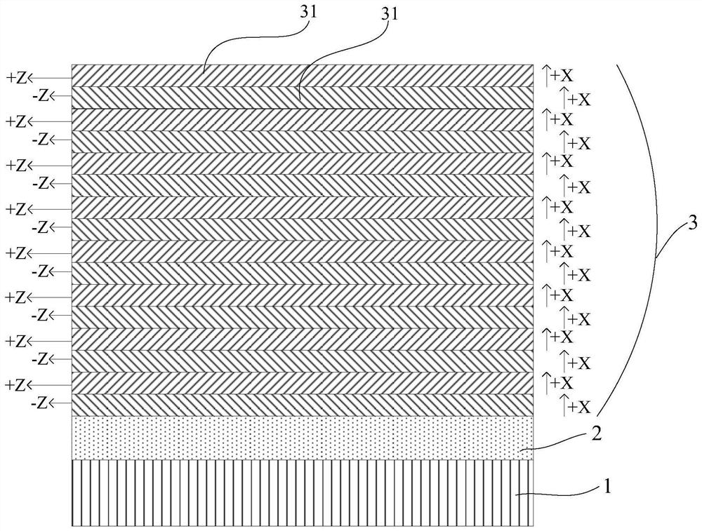
[0129] (1) The preparation is 4 inches, the thickness is 0.5 mm and has a smooth surface of the smooth surface, wherein the silicon wafer is less than 0.5 nm, and the silicon substrate is cleaned, and the CVD method is used. The smooth surface of the silicon wafer is alternately deposited 2 layers of silicon oxide layer and a 2 layer nitride layer, each layer of silicon oxide layer and a silicon nitride layer having a thickness of 200 nm, and the silicon oxide layer and a silicon nitride layer. Co-constituting the buffer layer;

[0130] (2) The preparation of X-cracked x-cut is a lithium tissue wafer (for ease of description, "the first crystal circle", the large cutting direction is + z-axis direction, and there is from the large cutting direction as the -Z-axis direction) , Use ion implantation method, from -X face ion ions (HE + ) Inject the first wafer, HE + The injection energy is 200KEV, the dose is 4 × 10 16 IONS / cm 2 , The first wafer is formed to form a thin film layer,...

Embodiment 2

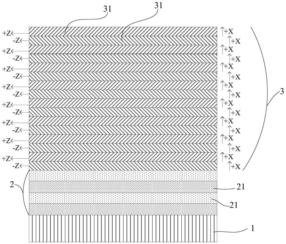
[0138] (1) The preparation is 4 inches, the thickness is 0.5 mm and has a single crystal silicon substrate wafer having a smooth surface, and after cleaning silicon substrate, the thermal oxidation method is used in the single crystal silicon substrate crystal circle process. 2 μm silica layer, wherein the silica surface roughness is less than 0.5 nm;

[0139] (2) The preparation of X-cracked x-cut is a lithium tissue wafer (for ease of description, "the first crystal circle", the large cutting direction is + z-axis direction, and there is from the large cutting direction as the -Z-axis direction) , Use ion implantation method, from -X face ion ions (HE + ) Inject the first wafer, HE + The injection energy is 20 keV, the dose is 1 × 10 17 IONS / cm 2 , The first wafer is formed to form a thin film layer, the separation layer, and the remaining material layer three-layer structure;

[0140] (3) When a plasma bonding method, the thin film layer of the first wafer-x-x surface after i...

Embodiment 3

[0148] (1) The first single crystal silicon substrate (for easy depicting, hereinafter referred to as "first substrate") is cleaned, and the first substrate is cleaned, and the first substrate is cleaned. A silica layer having a thickness of 2 μm is prepared by a thermoxing method in the process plane of the first substrate, wherein the silica surface roughness is less than 0.5 nm;

[0149] (2) The preparation of 4 inches of X-cut niobate wafers (for easy depicting, hereinafter referred to as "first wafer", the large cutting direction is + Z axis direction, away from the large cutting direction of -Z-axis direction), Using ion implantation, ion ions from -X face (HE + ) Inject the first wafer, HE + The injection energy is 1000 keV, the dose is 1 × 10 16 IONS / cm 2 , The first wafer is formed to form a thin film layer, the separation layer, and the remaining material layer three-layer structure;

[0150] (3) The thin film layer of the first wafer-x-x-x surface after plasma injecti...


PUM

PropertyMeasurementUnit
thicknessaaaaaaaaaa
angleaaaaaaaaaa
thicknessaaaaaaaaaa

Abstract

The present application provides a periodically polarized thin film substrate and a preparation method thereof. The periodically polarized thin film substrate includes a substrate (1), a buffer layer (2) and a piezoelectric single crystal layer (3) laminated in sequence, wherein , the piezoelectric single crystal layer (3) includes at least two piezoelectric single crystal sublayers (31), the polarization directions of adjacent piezoelectric single crystal sublayers (31) are opposite, obtained by bonding, the application provides The preparation method forms a periodically polarized thin film substrate by directly bonding multiple piezoelectric single crystal sublayers on the buffer layer. This method can be carried out at room temperature, and the process difficulty is low. The chemical cycle and the number of cycles can be flexibly controlled; effectively avoid the risk of breakdown caused by high voltage and the deterioration of surface quality caused by surface plating electrodes, and prevent light leakage into the substrate by setting a buffer layer, thereby reducing signal loss. The PPLN fabricated based on this substrate has completely through vertical domain walls.

Description

Technical field [0001] The present application belongs to the field of functional semiconductor materials, and more particularly to a periodic polarized thin film substrate and a preparation method thereof. Background technique [0002] Periodic Poled Ln, PPLN by quasi-phase matching technique (PPLN) is widely used in multiplier / decreasing, optical varieties oscillation, etc. In addition, in the field of optical communications, especially wavelength conversion, all-optical switching, in particular, in particular wavelength conversion, all-optical switching, also has broad application prospects. [0003] In lithium niobate, relative to oxygen ions (negative electrical), due to the position of lithium ion (positive electricity) and niobium ion (positive electricity), a special direction from positive electrodes to negative electricity is formed, along this direction along biotic acid The z-axis of the lithium crystal, that is, the + z-axis direction or the -z direction. If a volt...

Claims


Application Information

Patent Timeline
Patent Type & Authority Patents(China)
IPC IPC(8): H01L41/083H01L41/27H01L41/312
CPCH10N30/50H10N30/05H10N30/072
Inventor 王金翠张秀全朱厚彬李真宇张涛
Owner JINAN JINGZHENG ELECTRONICS
Why Eureka
Try Eureka