Silicon germanium film parallel transfer method applied to uncooled infrared focal plane

An uncooled infrared, transfer method technology, applied in the field of parallel transfer of silicon germanium thin films, can solve the problems of uneven ion energy and bonding surface morphology, different bonding strengths of bonding areas, and difficulty in adapting to array manufacturing, etc. The effect of expanding the range of sensitive materials, flexible and controllable thickness, and simple process equipment

Inactive Publication Date: 2014-07-02
NANJING UNIV OF SCI & TECH
View PDF3 Cites 0 Cited by
  • Summary
  • Abstract
  • Description
  • Claims
  • Application Information

AI Technical Summary

Problems solved by technology

[0004] When using ion-assisted direct bonding, often due to the inhomogeneity of ion energy and bonding surface morphology, the bonding strength of the bonding area varies, or even cannot be bonded.
Due to the existence of these problems, especially its high requirements for surface roughness (<0.2nmRMS), this bonding method can only be realized in the laboratory with corresponding equipment, and it is difficult to adapt to large-scale array manufacturing

Method used


Image

  • Silicon germanium film parallel transfer method applied to uncooled infrared focal plane
  • Silicon germanium film parallel transfer method applied to uncooled infrared focal plane
  • Silicon germanium film parallel transfer method applied to uncooled infrared focal plane

Examples


Embodiment Construction

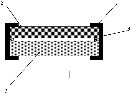
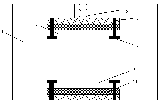
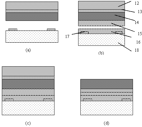
[0026] combine figure 1 , figure 2 with image 3 , the present invention is applied to the silicon germanium thin film parallel transfer bonding technology for the manufacture of uncooled infrared focal planes. Taking mr-i9100m glue and ULTRA-i300 glue as examples, the parallel transfer process is briefly described.

[0027] The process steps of using mr-i9100m glue are as follows:

[0028] Step 1: If image 3 As shown in the cleaning procedure in , follow the RCA1 procedure (mix 25% NH3 solution and deionized water in a ratio of 1 to 5, after boiling, add H2O2 in a ratio of 1 to 6, and then immerse the wafer in the solution for 10 minutes ) cleaning the SOI wafer 2 and the CMOS wafer 3, blowing them dry with nitrogen, and then placing them in an oven at 200° C. for 30 minutes; wherein the SOI wafer 2 sequentially includes a silicon support layer 12, a BOX layer 13, a silicon The germanium thin film 14 , the CMOS wafer includes metal electrodes 17 and CMOS circuits 18 , a...


PUM


Abstract

The invention discloses a silicon germanium film parallel transfer method applied to an uncooled infrared focal plane. The silicon germanium film parallel transfer method comprises the following steps of: cleaning wafers; gluing and pre-roasting the wafers; fixing the wafers by using a clamp to form a wafer pair; performing thermal compression bonding on the wafers; removing an SI supporting layer and a BOX layer; and the like. According to the silicon germanium film parallel transfer method, the problems of deposition conditions of a sensitive material and processing compatibility of the CMOS (Complementary Metal Oxide Semiconductor) wafers are not required to be considered; the silicon germanium / silicon quantum well material with deposition temperature of over 600 DEG C can be used; the range of the sensitive material capable of being used by the uncooled infrared focal plane can be expanded; a polishing process of a wafer bonding face is saved; the adhesion of the material after parallel transfer is also better, and the method is more suitable for large-scale production; and bonding glue is directly used as a sacrificial layer, both a coating process and a removal process of the bonding glue are simpler, and the thickness of the sacrificial layer is more flexible and controllable.

Description

technical field [0001] The invention belongs to the field of microelectronic processing technology applied to the manufacture of infrared imaging devices, in particular to a method for parallel transfer of silicon germanium thin films applied to uncooled infrared focal planes. Background technique [0002] Infrared imaging technology has a wide range of applications and demands in military and civilian fields. Infrared imaging reflects the information of thermal radiation on the surface of an object and its internal heat dissipation. It is an extension of people's vision beyond the visible light band and a new means of observing and perceiving the objective world. With the breakthrough of infrared sensitive material technology and the rapid development and maturity of MEMS (micro-electro-mechanical system) manufacturing technology, miniature bolometers have been widely used in military and civilian fields, such as thermal imaging cameras, night vision cameras, thermal Senso...

Claims


Application Information

Patent Timeline
Patent Type & Authority Patents(China)
IPC IPC(8): H01L21/02H01L21/18
Inventor 王开鹰董涛方中何勇杨朝初苏岩
Owner NANJING UNIV OF SCI & TECH
Why Eureka
Try Eureka