Thin film transistor and manufacturing method thereof, display substrate and display device

A technology of thin film transistor and manufacturing method, which is applied to transistors, semiconductor/solid-state device manufacturing, semiconductor device and other directions, can solve the problems of high production cost and long manufacturing cycle of thin film transistors, so as to reduce the production cost, shorten the manufacturing cycle, and reduce the patterning. The effect of the number of processes

Pending Publication Date: 2020-08-18
BOE TECH GRP CO LTD +1
View PDF3 Cites 0 Cited by
  • Summary
  • Abstract
  • Description
  • Claims
  • Application Information

AI Technical Summary

Problems solved by technology

[0002] In the prior art, more patterning processes are required to manufacture thin film transistors, resulting in a longer preparation cycle and higher production costs of thin film transistors

Method used


Image

  • Thin film transistor and manufacturing method thereof, display substrate and display device
  • Thin film transistor and manufacturing method thereof, display substrate and display device
  • Thin film transistor and manufacturing method thereof, display substrate and display device

Examples


Embodiment Construction

[0048] In order to make the technical problems, technical solutions and advantages to be solved by the embodiments of the present invention clearer, the following will describe in detail with reference to the drawings and specific embodiments.

[0049] Embodiments of the present invention provide a thin film transistor and its manufacturing method, a display substrate, and a display device, which can reduce the production cost of the thin film transistor.

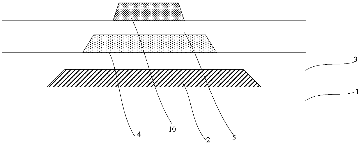
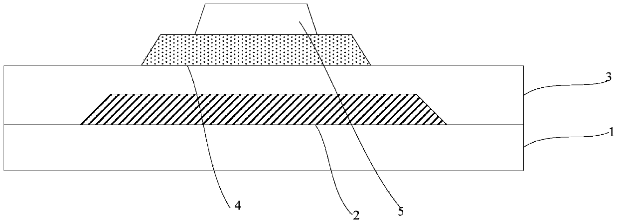
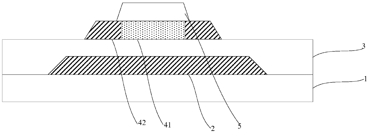
[0050] An embodiment of the present invention provides a method for manufacturing a thin film transistor, which uses a single patterning process to form a source, a drain, and a gate of the thin film transistor.

[0051] In this embodiment, the source, drain, and gate of the thin film transistor are formed by one patterning process, without the need to separately fabricate the source, drain, and gate of the thin film transistor through multiple patterning processes, which can reduce the patterning process for manufacturing t...


PUM

PropertyMeasurementUnit
thicknessaaaaaaaaaa

Abstract

The invention provides a thin film transistor and a manufacturing method thereof, a display substrate and a display device, and belongs to the technical field of display. According to the manufacturing method of the thin film transistor, a source electrode, a drain electrode and a grid electrode of the thin film transistor are formed through a one-time composition process. According to the technical scheme, the composition process times in manufacturing the thin film transistor can be reduced, and the production cost of the thin film transistor is reduced.

Description

technical field [0001] The present invention relates to the field of display technology, in particular to a thin film transistor, a manufacturing method thereof, a display substrate, and a display device. Background technique [0002] In the prior art, more patterning processes are required to manufacture thin film transistors, which results in a longer manufacturing cycle and higher production costs for thin film transistors. Contents of the invention [0003] The technical problem to be solved by the present invention is to provide a thin film transistor and its manufacturing method, a display substrate, and a display device, which can reduce the production cost of the thin film transistor. [0004] In order to solve the above technical problems, embodiments of the present invention provide technical solutions as follows: [0005] In one aspect, a method for manufacturing a thin film transistor is provided, which uses a single patterning process to form the source, drai...

Claims


Application Information

Patent Timeline
Patent Type & Authority Applications(China)
IPC IPC(8): H01L21/336H01L29/786
CPCH01L29/66742H01L29/78696
Inventor 丁远奎赵策胡迎宾宋威闫梁臣
Owner BOE TECH GRP CO LTD
Why Eureka
Try Eureka