Thin-film transistor array substrate and manufacturing method and electronic devices thereof

A transistor array and thin film field effect technology, applied in the field of liquid crystal display, can solve the problems of complex manufacturing process and high manufacturing cost, achieve high mobility, reduce manufacturing time, and reduce the number of patterning processes

Active Publication Date: 2014-06-25
BOE TECH GRP CO LTD
View PDF4 Cites 0 Cited by
  • Summary
  • Abstract
  • Description
  • Claims
  • Application Information

AI Technical Summary

Problems solved by technology

[0005] However, the manufacturing process of the existing transparent oxide TFT array substrate is relatively complicated, requiring at least four patterning processes to complete, resulting in high manufacturing costs

Method used


Image

  • Thin-film transistor array substrate and manufacturing method and electronic devices thereof
  • Thin-film transistor array substrate and manufacturing method and electronic devices thereof
  • Thin-film transistor array substrate and manufacturing method and electronic devices thereof

Examples


Embodiment Construction

[0061] In order to make the technical problems, technical solutions and advantages to be solved by the embodiments of the present invention clearer, the following will describe in detail with reference to the drawings and specific embodiments.

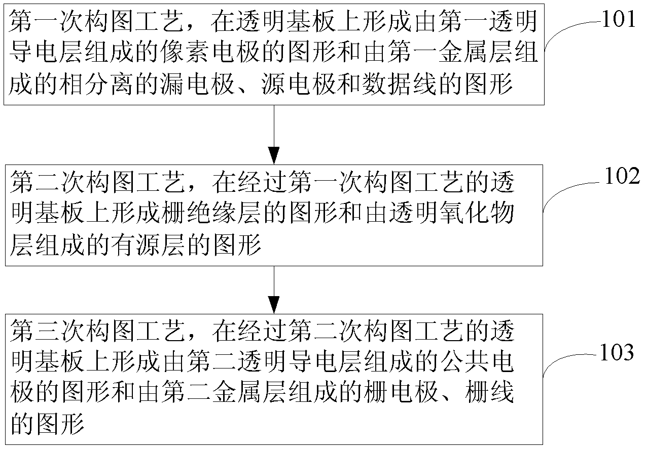
[0062] Embodiments of the present invention aim at the problems that the manufacturing process of the transparent oxide TFT array substrate is relatively complicated and the manufacturing cost is high in the prior art, and provide a thin film field effect transistor array substrate and its manufacturing method, and an electronic device, which adopts three-time patterning process that is The transparent oxide TFT array substrate can be produced, the manufacturing process of the transparent oxide TFT array substrate is simplified, the manufacturing time is shortened, and thus the production cost is reduced.

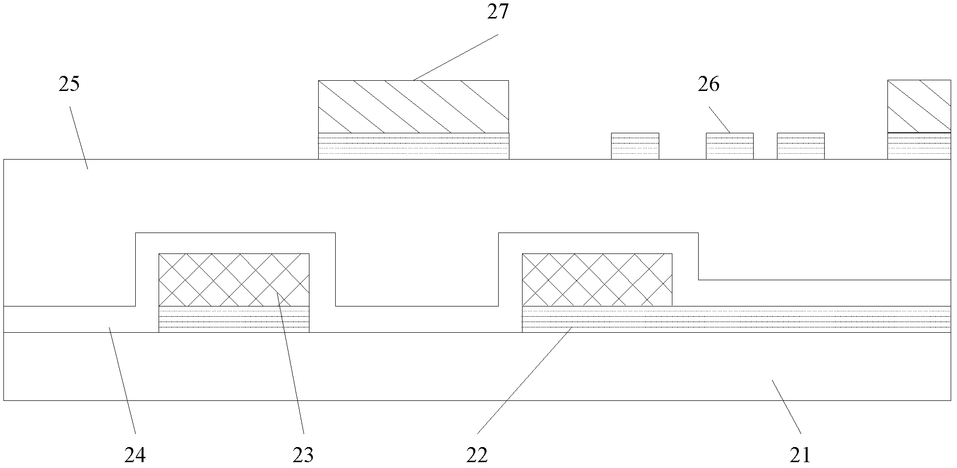
[0063] figure 1 It is a schematic flow diagram of a manufacturing method of a thin film field effect transistor array substrate ac...


PUM

PropertyMeasurementUnit
thicknessaaaaaaaaaa
thicknessaaaaaaaaaa
thicknessaaaaaaaaaa

Abstract

According to embodiments of the present invention, there are provided a TFT array substrate, a method for manufacturing the TFT array substrate and an electronic device. The method for manufacturing the TFT array substrate comprises: a first patterning process, in which a pattern of a pixel electrode formed by a first transparent conductive layer and patterns of a drain electrode and a source electrode that are separated from each other and a data line, which are formed by a first metal layer, are formed on a transparent substrate; a second patterning process, in which a pattern of a gate insulating layer and a pattern of an active layer formed by a transparent oxide layer are formed on the transparent substrate subjected to the first patterning process; and a third patterning process, in which a pattern of a common electrode formed by a second transparent conductive layer and patterns of a gate electrode and a gate line which are formed by a second metal layer are formed on the transparent substrate subjected to the second patterning process.

Description

technical field [0001] The invention relates to the field of liquid crystal display, in particular to a thin film field effect transistor array substrate, a manufacturing method thereof, and an electronic device. Background technique [0002] In the prior art, the vast majority of flat panel display devices are active matrix liquid crystal display devices (AMLCD). Since a-Si is easy to be prepared in a large area at low temperature and the technology is mature, it has become the most widely used technology at present. [0003] TFT (Thin Film Transistor, Thin Film Field Effect Transistor)-LCD (Liquid Crystal Display, liquid crystal display) is a kind of active matrix type liquid crystal display. According to the direction of the electric field driving the liquid crystal, TFT-LCD is divided into vertical electric field type, horizontal electric field type and multi-dimensional electric field type, while the vertical electric field type includes twisted nematic (TN) TFT_LCD, an...

Claims


Application Information

Patent Timeline
Patent Type & Authority Patents(China)
IPC IPC(8): H01L21/77H01L27/12G02F1/1362G02F1/1368
CPCH01L21/32139H01L27/1288H01L27/124H01L27/1225G02F2001/136236H01L27/127G02F2001/13629G02F1/136236G02F1/13629G02F1/1343
Inventor 宁策张学辉杨静
Owner BOE TECH GRP CO LTD
Why Eureka
Try Eureka