Array substrate, manufacturing method thereof, and display device

A technology for array substrates and manufacturing methods, which is applied in the display field, can solve problems such as complex manufacturing steps of array substrates, lower product yields, and high alignment accuracy, and achieve improved alignment misalignment, excellent electrical performance, and small parasitic capacitance Effect

Active Publication Date: 2017-01-25
BOE TECH GRP CO LTD
View PDF4 Cites 0 Cited by
  • Summary
  • Abstract
  • Description
  • Claims
  • Application Information

AI Technical Summary

Problems solved by technology

[0006] It is not difficult to find from the above-mentioned production methods that at least 8 to 9 patterning processes are required in the entire production process, and each patterning process needs to go through multiple processes such as gluing, exposure, development, cleaning, etc., which leads to arrays in the prior art. The manufacturing steps of the substrate are very complicated, and the production efficiency is low; in addition, high alignment accuracy is required in the patterning process, and high-precision alignment is very difficult. Once the alignment is not accurate, the yield rate of the product will directly decrease

Method used


Image

  • Array substrate, manufacturing method thereof, and display device
  • Array substrate, manufacturing method thereof, and display device
  • Array substrate, manufacturing method thereof, and display device

Examples


Embodiment 1

[0043] An embodiment of the present invention provides a method for manufacturing an array substrate, and the method includes the following steps:

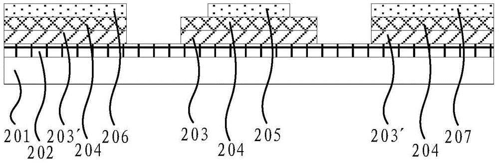
[0044] Step S11: sequentially form an active material layer, a gate insulating layer 204 and a metal thin film on the base substrate 201, and pattern the active material layer, gate insulating layer 204 and metal thin film through the first patterning process to form a The pattern of the source layer 203 and the pattern including the gate 205, the source 206, the drain 207, the gate line (not shown in the figure) and the data line (not shown in the figure), and the surrounding part of the gate 205 is exposed The gate insulating layer 204, the gate line or the data line is disconnected at the intersection of the gate line and the data line, such as figure 2 shown.

[0045] In this embodiment, the above step S11 may specifically include the following steps:

[0046] Step S111: sequentially forming an active material layer 501, a ...

Embodiment 2

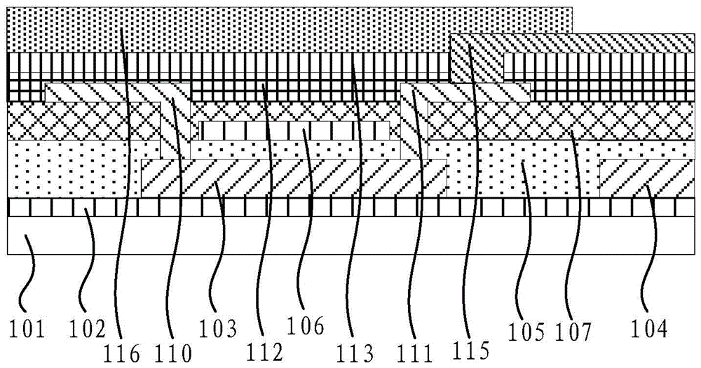
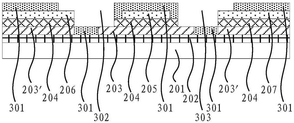
[0114] This embodiment provides an array substrate, such as Figure 17As shown, the array substrate provided in this embodiment includes: an active layer 203 on the base substrate 201; a gate insulating layer 204 covering the active layer 203; Gate 205, source 206, drain 207, gate line and data line, gate line or data line are disconnected at the intersection of gate line and data line; cover gate 205, source 206, drain 207 , the passivation layer 301 of the gate line and the data line; the source contact hole, the drain contact hole and the bridge structure contact hole located inside the passivation layer 301 and the gate insulating layer 204, and the source contact hole exposes part of the source electrode 206 and part of the active layer 203, the drain contact hole exposes part of the drain electrode 207 and part of the active layer 203, and the bridge structure contact hole exposes part of the disconnected gate line or data line; the source located in the same film layer ...

Embodiment 3

[0130] Based on the second embodiment, this embodiment provides a display device, which includes the array substrate described in the second embodiment.

[0131] The display device provided in this embodiment can preferably be an OLED (Organic Light Emitting Diode, organic light emitting diode) display device, such as: AMOLED (Active Matrix Organic Light Emitting Diode, active matrix organic light emitting diode) display device; it can also be LCD (Liquid Crystal Display, liquid crystal display device), such as: IPS (In-Plane Switching, in-plane switching) type LCD, etc.

[0132] In the display device provided by this embodiment, the gate and the source and drain of the TFT are in the same film layer, so there is no parasitic capacitance between the gate and the source and drain, thereby improving the performance of the display device.

[0133] Moreover, since the array substrate of the display device in this embodiment can be fabricated using fewer patterning processes, the p...


PUM

PropertyMeasurementUnit
thicknessaaaaaaaaaa
thicknessaaaaaaaaaa
thicknessaaaaaaaaaa

Abstract

The present invention provides an array substrate, a manufacturing method thereof, and a display device, wherein the manufacturing method includes: forming an active material layer, a gate insulating layer, and a metal thin film on the base substrate, and forming an array substrate through a first patterning process, including The pattern of the source layer and the pattern including the gate, source, drain, gate line and data line; form a passivation layer on the substrate, and form source contact holes and drain contact holes through the second patterning process and a bridge structure contact hole; a transparent conductive film is formed on the base substrate, and part of the transparent conductive film is removed by a film stripping process to form a source contact part, a drain contact part, a pixel electrode and a bridge structure. The above-mentioned manufacturing method reduces the number of use of the patterning process, and has the advantages of simple manufacturing method, high production efficiency, and high product yield.

Description

technical field [0001] The present invention relates to the field of display technology, in particular to an array substrate, a manufacturing method thereof, and a display device. Background technique [0002] Active matrix (Active Matrix) display device is a display device that uses thin film transistors (Thin Film Transistor, TFT for short) to drive pixel display. It has many advantages such as thinness, low power consumption, low radiation, and low cost. Mainstream display technology. [0003] Active matrix display devices all include a TFT array substrate. According to the different materials for the formation of the TFT active layer, the TFT array substrate can be divided into amorphous silicon (a-Si: H), low temperature polysilicon (Low Temperature Poly-Silicon, LTPS for short), high temperature polysilicon (High Temperature Poly-Silicon, HTPS for short), oxide semiconductor and other types. Among them, the LTPS TFT array substrate has become one of the research hots...

Claims


Application Information

Patent Timeline
Patent Type & Authority Patents(China)
IPC IPC(8): H01L21/77H01L27/12
CPCH01L27/124H01L27/1288H01L29/41733H01L29/41775H01L29/42356H01L29/42384H01L29/66757H01L29/78675H10K59/123H10K59/1216H10K59/1213H10K59/1201H10K59/122H01L27/1214H01L27/1218H01L27/1222H01L27/1248H01L27/1255H01L27/1274
Inventor 龙春平刘政王祖强任章淳
Owner BOE TECH GRP CO LTD
Why Eureka
Try Eureka