Wafer transmission monitoring method and wafer transmission monitoring device

A monitoring device and wafer technology, applied in the direction of conveyor objects, transportation and packaging, electrical components, etc., can solve the problem of semiconductor processing machine machine downtime, etc., to avoid abnormal transmission failure, avoid machine downtime, and reduce manpower The effect of loss of material resources

Inactive Publication Date: 2020-08-18
SHANGHAI GUONA SEMICON TECH CO LTD
View PDF0 Cites 3 Cited by
  • Summary
  • Abstract
  • Description
  • Claims
  • Application Information

AI Technical Summary

Problems solved by technology

[0005] The present invention provides a wafer transmission monitoring method and a wafer transmission monitoring device, which are used to solve the problem in the prior art that serious failures of the transmission structure easily lead to serious shutdown of the semiconductor processing machine, so as to improve the efficiency of the semiconductor machine. The production efficiency of the platform provides guarantee for the continuity and stability of production

Method used


Image

  • Wafer transmission monitoring method and wafer transmission monitoring device
  • Wafer transmission monitoring method and wafer transmission monitoring device
  • Wafer transmission monitoring method and wafer transmission monitoring device

Examples


Embodiment Construction

[0042] The specific implementations of the wafer transfer monitoring method and the wafer transfer monitoring device provided by the present invention will be described in detail below in conjunction with the accompanying drawings.

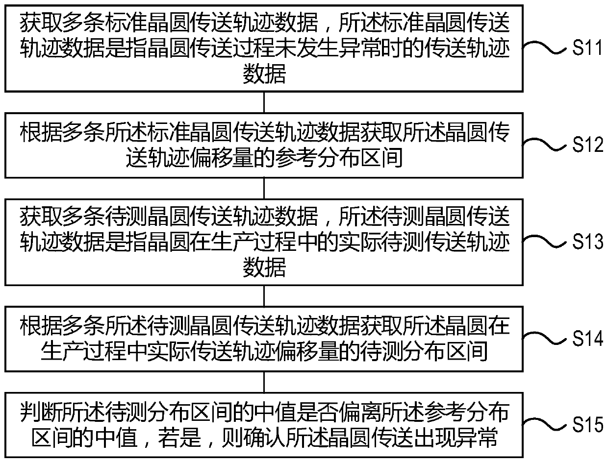
[0043] This specific embodiment provides a wafer transfer monitoring method, with figure 1 It is a flow chart of the wafer transfer monitoring method in the specific embodiment of the present invention. like figure 1 As shown, the wafer transmission monitoring method provided in this specific embodiment includes the following steps:

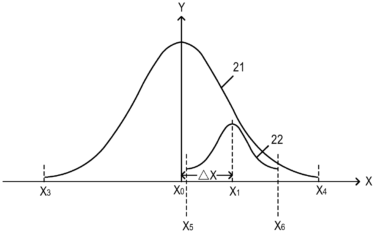
[0044] Step S11 , acquiring a plurality of pieces of standard wafer transfer trajectory data, where the standard wafer transfer trajectory data refers to the transfer trajectory data when no abnormality occurs during the wafer transfer process.

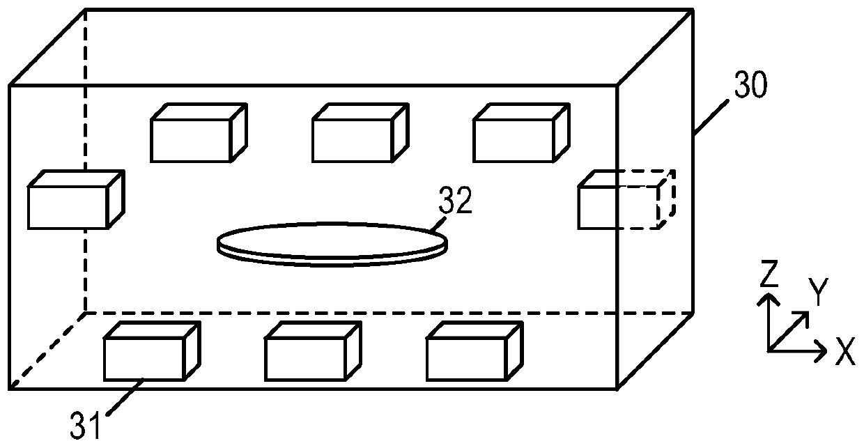
[0045] Specifically, in a semiconductor manufacturing process, a transfer structure such as a robot arm transfers wafers between multiple stations (ie, multiple machines f...


PUM


Abstract

The invention relates to a wafer transmission monitoring method and a wafer transmission monitoring device. The wafer transmission monitoring method comprises the following steps of acquiring the transmission track data of a plurality of standard wafers; obtaining a reference distribution interval of the wafer transmission track offset according to the plurality of pieces of standard wafer transmission track data; acquiring the transmission track data of a plurality of wafers to be tested; acquiring a to-be-measured distribution interval of the wafer transmission track offset according to theplurality of pieces of to-be-measured wafer transmission track data; and judging whether the median of the to-be-detected distribution interval deviates from the median of the reference distribution interval, and if so, determining that the wafer transmission is abnormal. According to the invention, the method achieves the prediction of the severe wafer transmission fault is predicted in advance,and the severe abnormal transmission fault caused by the accumulation of small wafer transmission faults is avoided.

Description

technical field [0001] The invention relates to the technical field of semiconductor manufacturing, in particular to a method for monitoring wafer transmission and a device for monitoring wafer transmission. Background technique [0002] Wafer refers to the silicon wafer used in the production of silicon semiconductor integrated circuits. Because its shape is generally set to a circle, it is called a wafer. Various circuit element structures can be processed on silicon wafers, thus becoming integrated circuit products with specific electrical functions. During the manufacturing process of semiconductor devices, it is often necessary to transfer wafers between different processing machines. For example, transfer devices such as EFEM (Equipment Front End Module, front-end transfer module) and vacuum transfer structures are used in semiconductor processing machines. The structure of the wafer. The transfer structure (such as a semiconductor industrial robot) is the core trans...

Claims


Application Information

Patent Timeline
Patent Type & Authority Applications(China)
IPC IPC(8): H01L21/67H01L21/677
CPCH01L21/67253H01L21/67259H01L21/67265H01L21/67703H01L21/67736
Inventor 毕迪
Owner SHANGHAI GUONA SEMICON TECH CO LTD
Why Eureka
Try Eureka