
Circuit board blue glue layer manufacturing method

A manufacturing method and circuit board technology, applied in the application of non-metallic protective layer, secondary treatment of printed circuit, etc., can solve the problems of affecting the adhesion strength of the board surface, rising production cost, easy falling off of blue glue, etc., to improve the adhesion. Attaching performance, improving quality, and precise effect of blue glue layer

Pending Publication Date: 2020-08-18
SHENZHEN SHIRUITAI TECH
View PDF0 Cites 0 Cited by
  • Summary
  • Abstract
  • Description
  • Claims
  • Application Information

AI Technical Summary

Problems solved by technology

[0009] The main disadvantages of this method are that due to the high viscosity of the blue glue, air bubbles will be produced after it is made by screen printing and dried, which will affect its adhesion to the board surface. Afterwards, the blue glue is easy to fall off and seep into tin, and the air bubbles and pits on the surface of the blue glue are prone to problems such as hidden tin. In addition, the price of the blue glue is relatively high, which increases the production cost of the product

Method used


Image

  • Circuit board blue glue layer manufacturing method
  • Circuit board blue glue layer manufacturing method
  • Circuit board blue glue layer manufacturing method

Examples


Embodiment Construction

[0036] The following will clearly and completely describe the technical solutions in the embodiments of the present invention with reference to the accompanying drawings in the embodiments of the present invention. Obviously, the described embodiments are some of the embodiments of the present invention, but not all of them. Based on the embodiments of the present invention, all other embodiments obtained by persons of ordinary skill in the art without making creative efforts belong to the protection scope of the present invention.

[0037] It should be understood that when used in this specification and the appended claims, the terms "comprising" and "comprises" indicate the presence of described features, integers, steps, operations, elements and / or components, but do not exclude one or Presence or addition of multiple other features, integers, steps, operations, elements, components and / or collections thereof.

[0038] It should also be understood that the terminology used ...


PUM

PropertyMeasurementUnit
thicknessaaaaaaaaaa
thicknessaaaaaaaaaa

Abstract

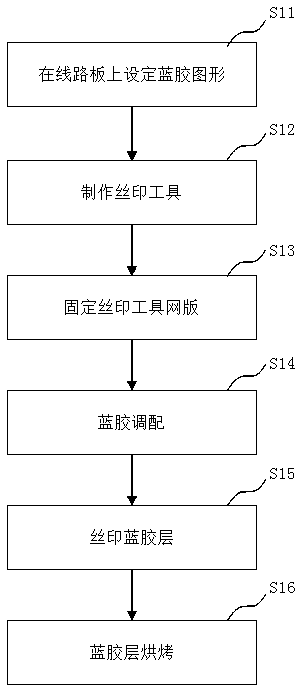
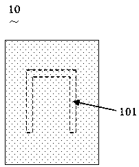
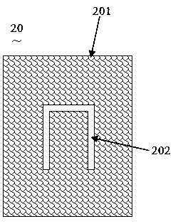
The invention discloses a circuit board blue glue layer manufacturing method. The method comprises the following steps: setting a blue glue pattern on a circuit board, manufacturing a printed patternby adopting a flat plate, adhering the printed pattern plate and a silk-screen printing plate to form a printing tool screen printing plate, preparing compound blue glue by utilizing peelable blue glue and white character ink, and performing vacuum baking on a blue glue layer after printing the compound blue glue. Gauze is replaced by a flat plate, the peelable blue glue and white character ink are blended to form novel blue glue ink, and then printing and vacuum baking are performed, so that the problems of poor bonding force, overlarge deviation, surface pinhole bubbles, blue glue layer falling, tinning, low manufacturing efficiency and the like of a blue glue protective layer generated by pasting high-temperature-resistant adhesive tape and silk-screen printing blue glue are effectivelysolved.

Description

technical field [0001] The invention relates to the technical field of electronic manufacturing, in particular to a method for manufacturing a blue glue layer of a circuit board. Background technique [0002] Hot air leveling, commonly known as tin spraying, is one of the surface treatment processes of circuit boards. Its working principle is to immerse the circuit boards to be made into tin pads into a molten tin furnace, and use hot air to remove the circuit boards from the tin furnace at the same time. The excess tin material on the surface of the circuit board and in the hole is blown off, and the remaining solder evenly covers the surface of the pad to form a tin pad. [0003] For the surface of the same circuit board, one kind of surface treatment is first performed on part of the pads, and then the double surface treatment method is used to make hot air leveling on the other part of the pads. After the first surface treatment, a protective layer is required. Protect ...

Claims


Application Information

Patent Timeline
Patent Type & Authority Applications(China)
IPC IPC(8): H05K3/28
CPCH05K3/28
Inventor 刘会敏
Owner SHENZHEN SHIRUITAI TECH
Learn More