daf film and its preparation method, chip packaging structure

A chip and support technology, applied in the field of semiconductor packaging, can solve problems such as chip and DAF film tilt, uneven force on the chip, and affect the quality of chip packaging, so as to improve quality and efficiency and prevent chip tilt.

Active Publication Date: 2022-06-07
NANTONG TONGFU MICROELECTRONICS CO LTD
View PDF0 Cites 0 Cited by
  • Summary
  • Abstract
  • Description
  • Claims
  • Application Information

AI Technical Summary

Problems solved by technology

During the film loading process, it is difficult to control the level of the chip due to the influence of factors such as hand equipment and fixtures
For example: if figure 1 As shown, since the chip 22 is bonded to the substrate 33 through the DAF film 11 after the suction nozzle sucks the chip, during the chip loading process, when the suction nozzle is in partial contact with the chip, a pressure F is applied to the chip, resulting in uneven force on the chip, resulting in chip There is an inclination between the DAF film and the chip packaging quality

Method used


Image

  • daf film and its preparation method, chip packaging structure
  • daf film and its preparation method, chip packaging structure
  • daf film and its preparation method, chip packaging structure

Examples


Embodiment Construction

[0033] The present application will be further described in detail below in conjunction with the accompanying drawings and embodiments. It will be appreciated that the specific embodiments described herein are used only to explain the invention in question and not to qualify the invention. It should also be noted that, in order to facilitate the description, only a portion of the invention is shown in the drawings.

[0034] It should be noted that, in the absence of conflict, the embodiments in the present application and the features in the embodiments may be combined with each other. The present application will be described below with reference to the accompanying drawings and in conjunction with embodiments.

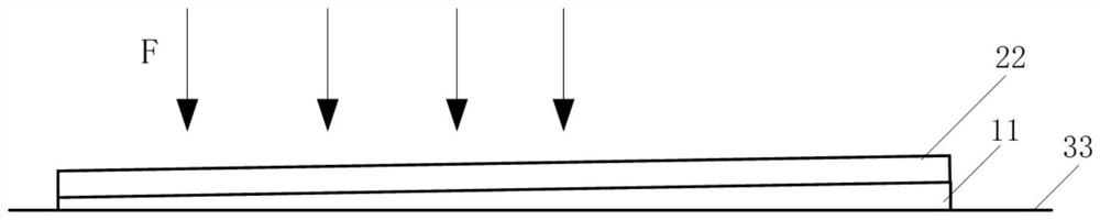
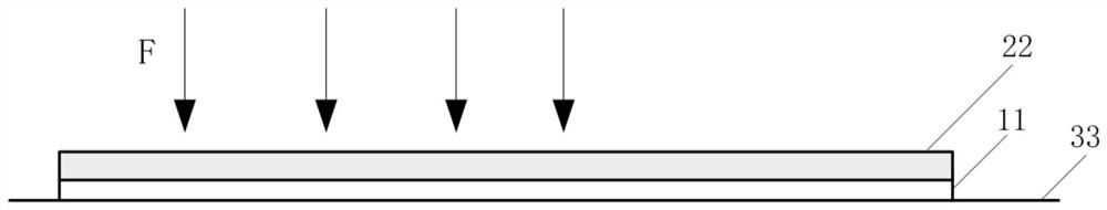
[0035] The chip and DAF film are bonded together as DAF patches, and existing DAF patches can be bonded directly to the substrate due to the DAF film on the back of the chip. However, during the bonding process of the existing DAF film, the chip is tilted relative to the...


PUM

PropertyMeasurementUnit
melting pointaaaaaaaaaa

Abstract

The application discloses a DAF film, its preparation method, and a chip packaging structure. The DAF film includes a first rubber surface, a second rubber surface, and an intermediate high thermal conductivity layer. A support body is arranged in the intermediate high thermal conductivity layer to prevent The chip is tilted. In this application, by adding a support body to the DAF film, the support body provides effective support to ensure that when the chip is pressed against the DAF film, the chip is prevented from tilting due to uneven force. The DAF film of the present invention, through the addition of a support body, realizes that the chip is always kept level when loading the chip, and does not change its own adhesiveness, and can be used for high-speed wafer bonding processing, improving the quality and efficiency of chip packaging.

Description

Technical field [0001] The present invention relates generally to the field of semiconductor packaging technology, specifically to a DAF film and a preparation method thereof, a chip packaging structure. Background [0002] In the chip packaging process, DAF film (Die attach film) is a commonly used key material. DAF film is used for laser cutting during chip packaging, the wafer can be cut and separated together, peeled off, so that the cutting of the wafer (Die), can also be adhered to the film, will not cause scattered arrangement due to cutting. During wafer bonding, after suctioning through the nozzle, it is bonded to the substrate through the DAF membrane. [0003] The existing DAF film comprises a first rubber surface, a second rubber surface and an intermediate layer of high thermal conductivity resin layer, the first rubber surface is bonded to the chip, and the second rubber surface is bonded to the substrate. In the process of film loading, the influence of hand equipm...

Claims


Application Information

Patent Timeline
Patent Type & Authority Patents(China)
IPC IPC(8): C09J7/22H01L21/683
CPCC09J7/22H01L21/6836C09J2203/326C09J2400/226
Inventor 任济平
Owner NANTONG TONGFU MICROELECTRONICS CO LTD
Why Eureka
Try Eureka