Loading type waveguide optical modulator

A technology of modulator and waveguide light, which is applied in optics, instruments, optical components, etc., to achieve the effect of high modulation sensitivity and large modulation depth

Inactive Publication Date: 2020-09-04
金华伏安光电科技有限公司
View PDF0 Cites 1 Cited by
  • Summary
  • Abstract
  • Description
  • Claims
  • Application Information

AI Technical Summary

Problems solved by technology

However, there are few optical modulators based on loaded waveguides. Designing optical modulators based on loaded waveguides is of gre

Method used


Image

  • Loading type waveguide optical modulator
  • Loading type waveguide optical modulator
  • Loading type waveguide optical modulator

Examples


Embodiment 1

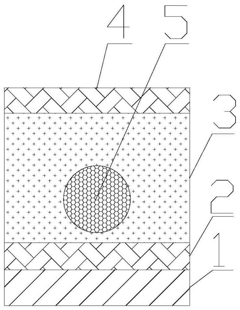
[0021] The invention provides a loaded waveguide light modulator. like figure 1 As shown, the optical modulator includes a substrate 1 , a first metal layer 2 , an electrostrictive material layer 3 , a second metal layer 4 , and a waveguide 5 . The material of the substrate 1 can be silicon or silicon dioxide. The material of the substrate 1 can also be other materials to facilitate the integration of the light modulator with other systems. The waveguide 5 is in the shape of a straight line, figure 1 The middle is the cross section of the waveguide 5 . The first metal layer 2 is placed on the substrate 1 . At the interface between the first metal layer 2 and the electrostrictive material layer 3, the first metal layer 2 is a plane. The material of the first metal layer 2 is gold. A layer 3 of electrostrictive material is placed on the first metal layer 2 . The electrostrictive material layer 3 can be any electrostrictive material, preferably, the material of the electro...

Embodiment 2

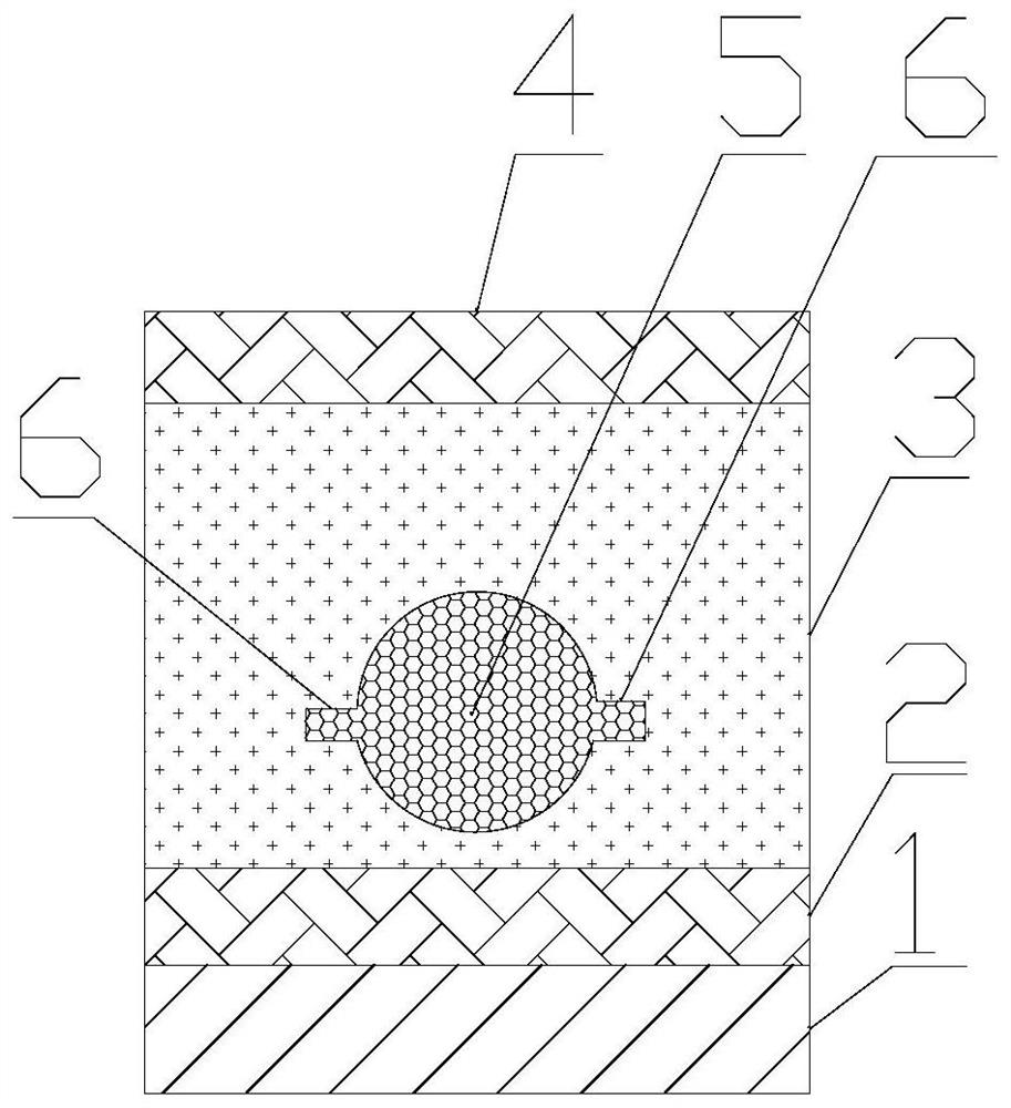
[0026] On the basis of Example 1, such as figure 2 As shown, a protruding portion 6 is also provided on the side of the waveguide portion 5 . The protruding part 6 is rectangular, and the long side of the rectangle is along the horizontal direction. The protruding part 6 makes the waveguide part 5 subjected to more effects of the electrostrictive material layer 3 to generate more deformation and change the propagation characteristics of the loaded waveguide more. For example, when the electrostrictive material layer 3 stretches, figure 2 The electrostrictive material under the middle protrusion will act on the protrusion 6, so that the waveguide receives more upward force, thereby generating more upward displacement.

Embodiment 3

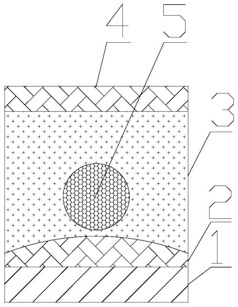
[0028] On the basis of Example 2, such as image 3 As shown, the interface between the first metal layer 2 and the electrostrictive material layer 3 has a convex arc surface, and the top of the arc surface is located directly below the waveguide part 5 . In this way, when a voltage is applied between the first metal layer 2 and the second metal layer 4, for the first metal layer 2, the charge is more concentrated on the top of the arc surface, and the top of the arc surface is in contact with the guided wave. The distance between the parts 5 is smaller, so that more charges of opposite sign are induced on the waveguide part 5 . Under the combined action of the charges on the arc surface of the first metal layer 2 and the charges of opposite sign on the waveguide 5, a stronger electric field is formed between the arc surface of the first metal layer 2 and the waveguide 5, and these electric fields make The electrostrictive material in between produces more deformation, thereby...


PUM


Abstract

The invention provides a loading type waveguide optical modulator, which is characterized in that an electrostrictive material layer is arranged between a first metal layer and a second metal layer, wherein a wave guide part is arranged in the electrostrictive material layer, and a loaded waveguide is formed between the first metal layer and the wave guide part. During application, an electric field is applied to the first metal layer and the second metal layer, wherein the electrostrictive material layer deforms, so that the distance between the first metal layer and the wave guide part is changed, and the propagation characteristic of the waveguide is changed. In the invention, because the propagation characteristic of the loaded waveguide is very sensitive to the distance, the loaded waveguide has the advantages of high modulation sensitivity and large modulation depth, and has an important application prospect in the field of loaded waveguide optical modulation.

Description

technical field [0001] The invention relates to the field of optical modulators, in particular to a loaded waveguide optical modulator. Background technique [0002] The loaded waveguide includes a metal film and a high-refractive-index medium, and electromagnetic wave energy is confined to propagate between the metal film and the high-refractive-index medium. The loaded waveguide has the advantages of small mode area and long propagation distance. However, there are few optical modulators based on loaded waveguides. Designing optical modulators based on loaded waveguides is of great significance for information loading and high-sensitivity sensing, and is of great value for enriching micro-nano photonics devices. Contents of the invention [0003] In order to solve the above problems, the present invention provides a loaded waveguide optical modulator, which includes a substrate, a first metal layer, an electrostrictive material layer, a second metal layer, and a wavegui...

Claims


Application Information

Patent Timeline
IPC IPC(8): G02B26/00
CPCG02B26/00
Inventor 不公告发明人
Owner 金华伏安光电科技有限公司
Why Eureka
Try Eureka