Check patentability & draft patents in minutes with Patsnap Eureka AI!

3d NAND flash memory device and its integration method

A flash memory, flash storage technology, applied in read-only memory, static memory, digital memory information and other directions, can solve the problems of unsatisfactory SLCNAND read/write performance, reduce storage density, and increase SSD cost.

Active Publication Date: 2021-10-01
YANGTZE MEMORY TECH CO LTD
View PDF6 Cites 0 Cited by
  • Summary
  • Abstract
  • Description
  • Claims
  • Application Information

AI Technical Summary

Problems solved by technology

However, the 3D TLC NAND flash memory utilized by the above combined structure reduces the storage density and increases the cost of SSD
In addition, the read / write performance of SLC NAND with combined structure is not satisfactory

Method used


Image

  • 3d NAND flash memory device and its integration method
  • 3d NAND flash memory device and its integration method
  • 3d NAND flash memory device and its integration method

Examples


Embodiment Construction

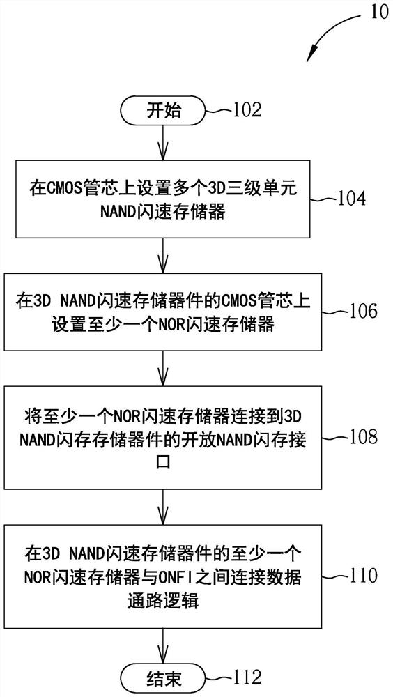
[0009] figure 1 is a schematic diagram of an integration process 10 for a 3D NAND flash memory device according to an embodiment of the present invention. An integrated process 10 for a 3D NAND flash memory device includes the following steps:

[0010] Step 102: start.

[0011] Step 104: Place a plurality of 3D triple-level cell (TLC) NAND flash memories on a CMOS die.

[0012] Step 106: disposing at least one NOR flash memory on the CMOS die of the 3D NAND flash memory device.

[0013] Step 108: Connect the at least one NOR flash memory to an Open NAND Flash Interface (ONFI) of the 3D NAND flash memory device.

[0014] Step 110: Connect a data path logic unit between the at least one NOR flash memory of the 3D NAND flash memory device and the ONFI.

[0015] Step 112: end.

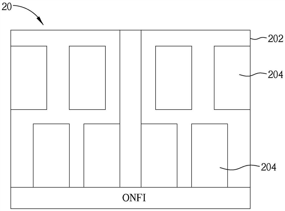
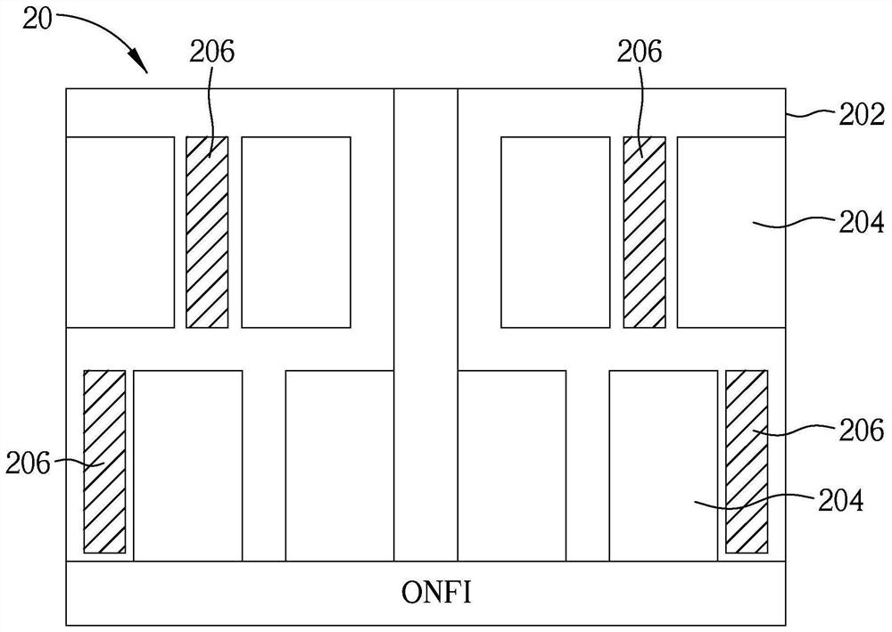
[0016] For an explanation of the integrated process 10, please also refer to figure 2 and image 3 , figure 2 and image 3 is a schematic diagram of a 3D NAND flash memory device 20 applying an ...


PUM


Abstract

An integration method for a 3D NAND flash memory device includes: disposing a plurality of 3D triple-level cell (TLC) NAND flash memories on a CMOS die; disposing at least one on the CMOS die of the 3D NAND flash memory device NOR flash memory; and the open NAND flash memory interface (ONFI) that described at least one NOR flash memory is connected to 3D NAND flash memory device; Wherein, described at least one NOR flash memory is arranged on the unused of CMOS die area.

Description

technical field [0001] The present invention relates to a 3D NAND flash memory device and an integration method thereof, and more particularly, to a 3D NAND flash memory device capable of improving storage space and read / write performance and an integration method thereof. Background technique [0002] In order to provide better performance of solid state disks (SSDs), a combined structure of single-level cell (SLC) NAND flash memory and 3D triple-level cell (TLC) NAND flash memory is widely utilized in conventional SSD implementations. Hot data that is frequently read / written is stored in SLC NAND flash, and cold data that is infrequently read / written is stored in 3D TLC NAND flash. However, the 3D TLC NAND flash memory utilized by the above combined structure reduces the storage density and increases the cost of the SSD. In addition, the read / write performance of SLC NAND with combined structure is not satisfactory. Therefore, it is necessary to make improvements to the ...

Claims


Application Information

Patent Timeline
Patent Type & Authority Patents(China)
IPC IPC(8): H01L27/11529H01L27/11553H01L27/11573H01L27/11578G11C16/04H10B41/41H10B41/10H10B41/20H10B41/23H10B41/27H10B41/35H10B43/10H10B43/20H10B43/27H10B43/35H10B43/40
CPCG11C16/0483G11C5/06G06F3/0608G11C11/5628G11C16/10G06F3/0688G11C11/5642G11C11/5671G11C11/005G11C16/0408G11C16/26G11C5/02H01L27/0207H10B41/41H10B41/10H10B41/35H10B41/23H10B41/20H10B41/27H10B43/35H10B43/10H10B43/20H10B43/40H10B43/27
Inventor 顾沂侯春源李跃平陈嘉伟
Owner YANGTZE MEMORY TECH CO LTD
Features
  • R&D
  • Intellectual Property
  • Life Sciences
  • Materials
  • Tech Scout
  • Unparalleled Data Quality
  • Higher Quality Content
  • 60% Fewer Hallucinations
Learn More