Chip-on-film packaging structure
A thin-film-on-chip packaging, thin-film technology, applied in electrical components, electrical solid-state devices, circuits, etc., can solve problems such as large film area
- Summary
- Abstract
- Description
- Claims
- Application Information
AI Technical Summary
Problems solved by technology
Method used
Image
Examples
Embodiment Construction
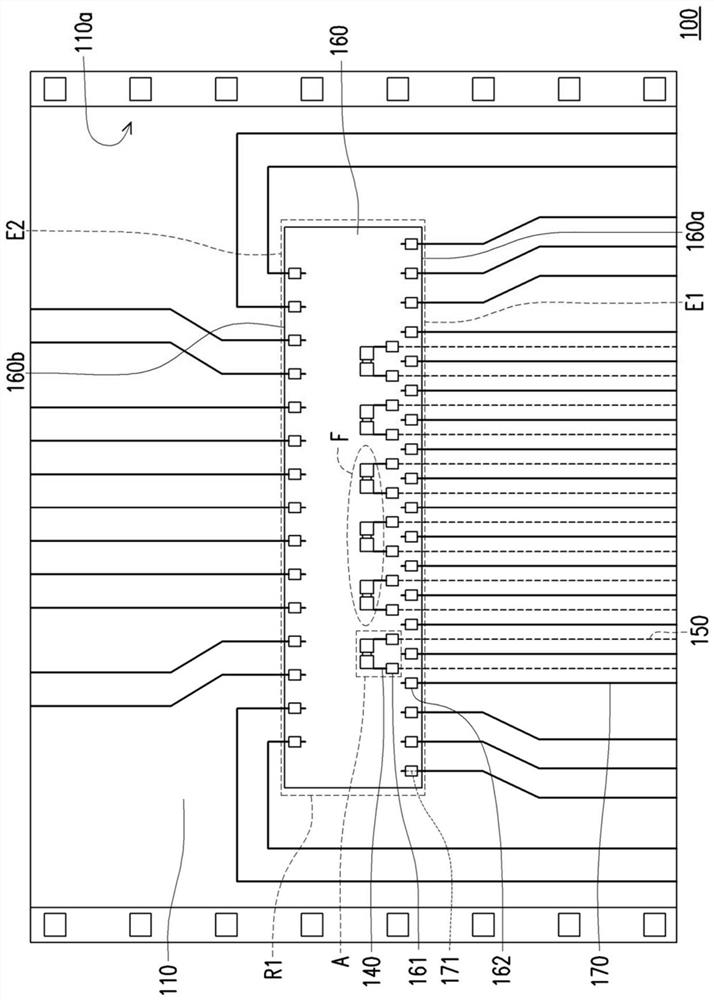
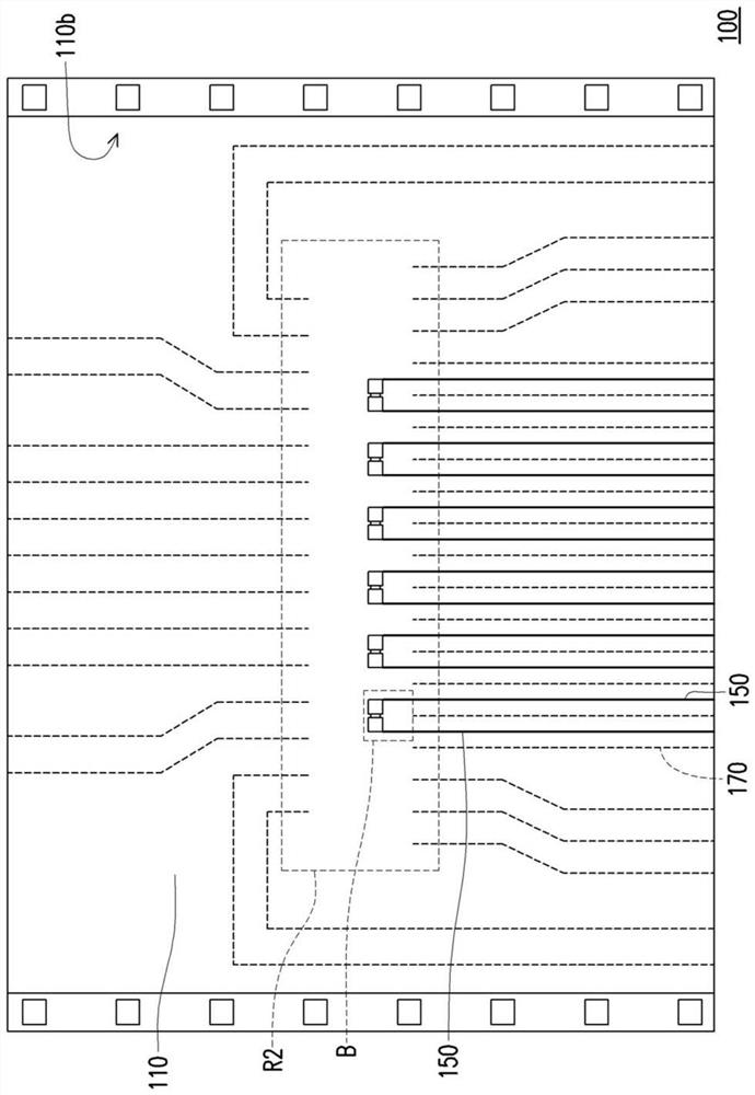
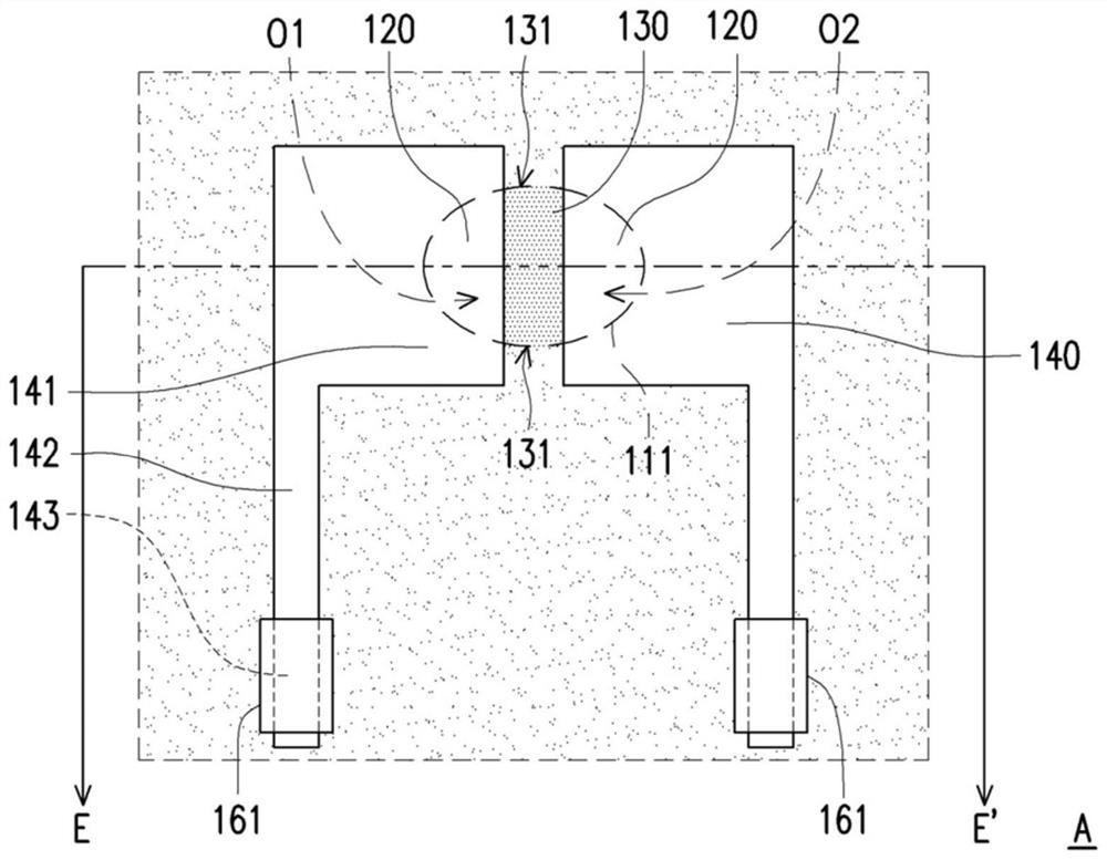
[0051] Figure 1A is a schematic top view of a chip-on-film packaging structure according to an embodiment of the present invention. Figure 1B yes Figure 1A Schematic bottom view of the thin film chip-on-chip packaging structure. Figure 1C yes Figure 1A An enlarged schematic view of region A of . Figure 1D yes Figure 1B An enlarged schematic view of region B of . Figure 1E yes Figure 1C Schematic cross-sectional view along section line E-E'. Figure 1F yes Figure 1A An enlarged schematic view of region F of . In order to clearly show the connection relationship between the chip 160 and the first upper pin 140, Figure 1A The chip 160 is rendered in perspective.
[0052] Please refer to Figure 1A to Figure 1F , in this embodiment, the film-on-chip packaging structure 100 includes a flexible film 110 , at least two conductive elements 120 , an insulator 130 , at least two first upper leads 140 , at least two lower leads 150 and a chip 160 . The flexible film 110...
PUM
 Abstract
Description
Claims
Application Information


