Method for improving circuit board test alignment and circuit board

A technology for circuit boards and alignment targets, which is applied in printed circuits, multilayer circuit manufacturing, printed circuit manufacturing, etc., can solve the problems of positioning hole position offset, low test efficiency, and insufficient accuracy.

Inactive Publication Date: 2020-10-27
珠海市鼎协电子有限公司
View PDF7 Cites 0 Cited by
  • Summary
  • Abstract
  • Description
  • Claims
  • Application Information

AI Technical Summary

Problems solved by technology

[0002] At present, the test positioning holes of circuit boards are generally made by drilling. After the positioning holes are drilled in the drilling process, in the subsequent copper plating process, due to the expansion and contraction of the material, the position of the positioning holes Misalignment occurs. When the circuit pattern is made, the alignment error between the film and the positioning hole causes the precision change between the circuit pattern and the positioning hole. Therefore, for the dense circuit board, when the circuit board is tested, due to the positioning The accuracy between the hole and the circuit pattern is not high enough, the test probe cannot accurately contact the pad, and repeated debugging is required, and the test efficiency is low

Method used


Image

  • Method for improving circuit board test alignment and circuit board
  • Method for improving circuit board test alignment and circuit board

Examples


Embodiment Construction

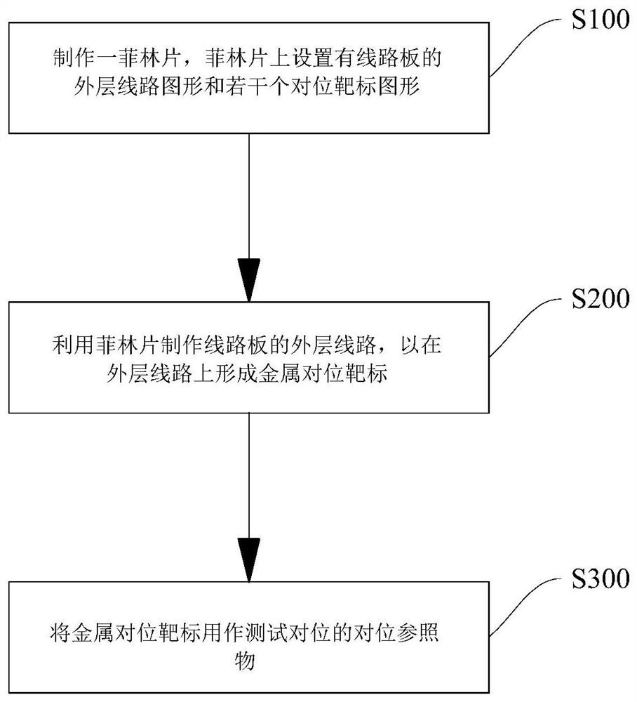
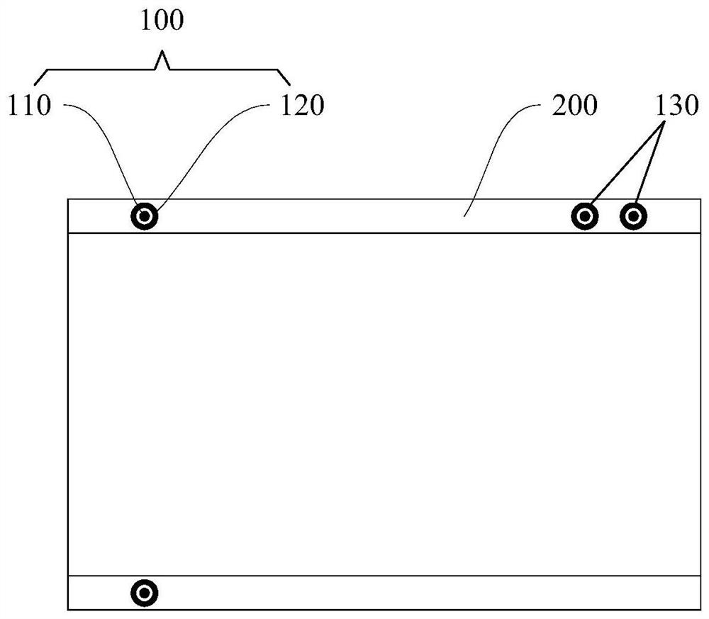
[0023] Embodiments of the present invention are described in detail below, examples of which are shown in the drawings, wherein the same or similar reference numerals designate the same or similar elements or elements having the same or similar functions throughout. The embodiments described below by referring to the figures are exemplary only for explaining the present invention and should not be construed as limiting the present invention.

[0024] In the description of the present invention, several means one or more, and multiple means two or more. Greater than, less than, exceeding, etc. are understood as not including the original number, and above, below, within, etc. are understood as including the original number. If the description of the first and second is only for the purpose of distinguishing the technical features, it cannot be understood as indicating or implying the relative importance or implicitly indicating the number of the indicated technical features or i...


PUM


Abstract

The invention discloses a method for improving the test alignment of a circuit board and the circuit board. The method comprises the steps of manufacturing a film, wherein the film is provided with anouter circuit pattern of the circuit board and a plurality of alignment target patterns; manufacturing an outer-layer circuit of the circuit board by using the film so as to form a metal alignment target on the outer-layer circuit; and using the metal alignment target as an alignment reference object for test alignment. The outer-layer circuit pattern and the metal alignment target of the circuitboard are synchronously manufactured by using the film, so that the position deviation between the outer-layer circuit pattern and the metal alignment target can be avoided, the test alignment precision of the circuit board is improved, repeated debugging during testing is avoided, and the test efficiency is improved.

Description

technical field [0001] The invention relates to the technical field of circuit boards, in particular to a method for improving the test alignment of circuit boards and the circuit board. Background technique [0002] At present, the test positioning holes of circuit boards are generally made by drilling. After the positioning holes are drilled in the drilling process, in the subsequent copper plating process, due to the expansion and contraction of the material, the position of the positioning holes Misalignment occurs. When the circuit pattern is made, the alignment error between the film and the positioning hole causes the precision change between the circuit pattern and the positioning hole. Therefore, for the dense circuit board, when the circuit board is tested, due to the positioning The precision between the hole and the circuit pattern is not high enough, the test probe cannot accurately contact the pad, repeated debugging is required, and the test efficiency is low....

Claims


Application Information

Patent Timeline
Patent Type & Authority Applications(China)
IPC IPC(8): H05K3/46H05K1/02H05K3/00
CPCH05K1/0266H05K3/0047H05K3/4638H05K2203/166
Inventor 刘超唐文波李永正
Owner 珠海市鼎协电子有限公司
Why Eureka
Try Eureka