LED chip packaging process

A technology of LED chips and packaging technology, which is applied in the direction of electrical components, electrical solid devices, circuits, etc., and can solve problems such as yellow edges, weak light efficiency, and phosphor powder settling to the bottom of the four sides

Active Publication Date: 2020-11-20
广东安珂光电科技有限公司
View PDF4 Cites 2 Cited by
  • Summary
  • Abstract
  • Description
  • Claims
  • Application Information

AI Technical Summary

Problems solved by technology

The packaged LED chip has single-side (top) light-emitting and multi-side light-emitting types. For multi-side light-emitting LED chips, it is necessary to coat the four sides and the top surface with fluorescent glue, but coat five light-emitting surfaces at the same time. During the flat curing process, it is easy for the phosphor to settle to the bottom of the four sides, resulting in uneven light output, weak light effect, and yellow edges at the bottom, which seriously affect product quality

Method used


Image

  • LED chip packaging process
  • LED chip packaging process
  • LED chip packaging process

Examples


Embodiment Construction

[0023] The scheme of this application is further described in conjunction with the accompanying drawings as follows:

[0024] A packaging process for LED chips, comprising the following steps:

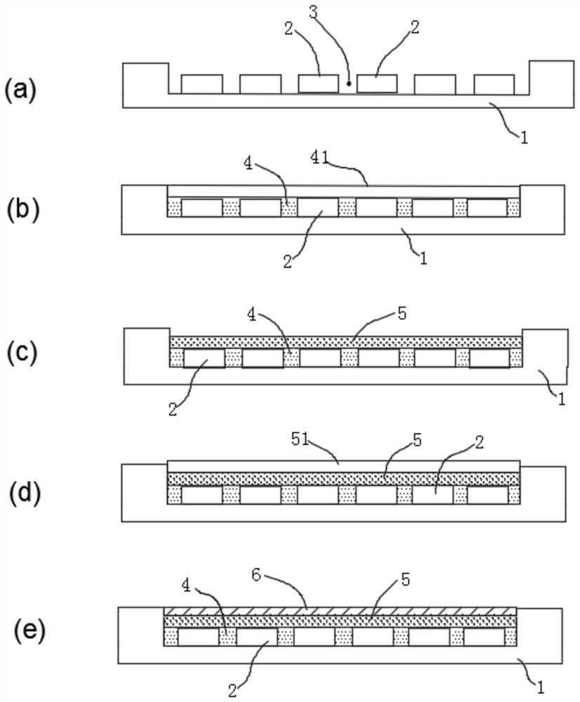
[0025] S1, see figure 1 As shown in figure (a), a carrier 1 and a matrix array of LED chips 2 arranged on the carrier 1 are provided, and there are gaps 3 between adjacent LED chips 2 .

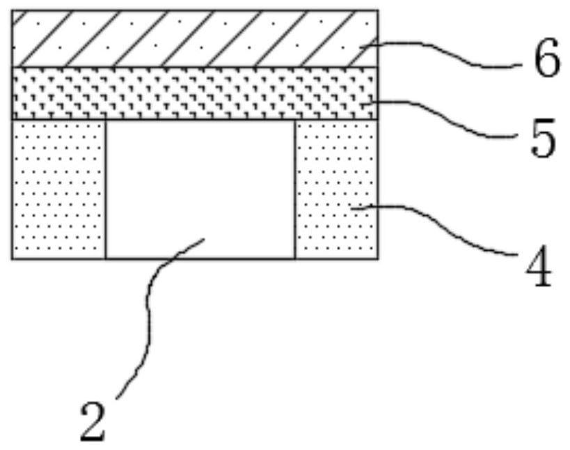
[0026] S2, see figure 1 As shown in the figure (b), the gap 3 is filled with the anti-sedimentation fluorescent glue 4, and the thickness of the anti-settling fluorescent glue 4 is controlled to be flush with the top surface of the LED chip 2, and the anti-settling fluorescent glue 4 is dried and cured. Glue 4. Specifically, do the following:

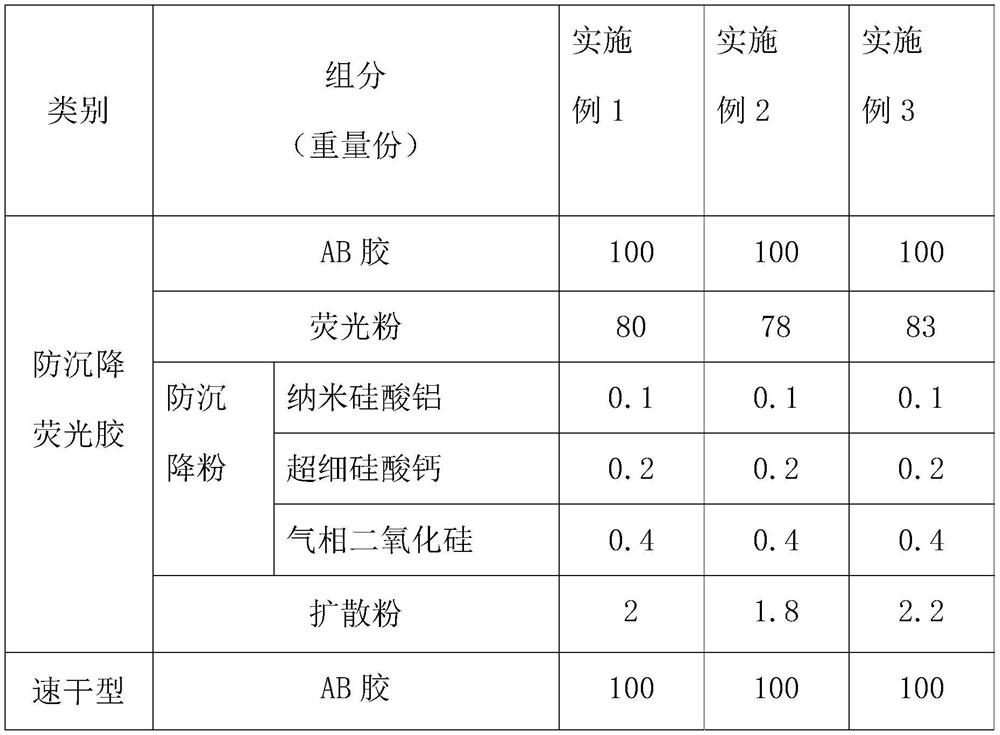
[0027] S2.1. Coating the anti-sedimentation fluorescent glue 4 on the matrix array of LED chips 2, the anti-sedimentation fluorescent glue 4 consists of 85-115 parts by weight of AB glue, 76-83 parts by weight of phosphor powder, 0.3- It is prepared by mix...


PUM


Abstract

The invention provides an LED chip packaging process, which comprises the following steps of: S1, providing a carrier and a matrix array of LED chips arranged on the carrier, and forming a gap betweenadjacent LED chips; S2, filling the gap with anti-settling fluorescent glue, controlling the thickness of the anti-settling fluorescent glue to be flush with the top surface of the LED chip, and drying and curing the anti-settling fluorescent glue; S3, coating the matrix array of the LED chip with quick-dry fluorescent glue to cover the top surface of the LED chip, and drying and curing the quick-dry fluorescent glue; S4, compounding an AB glue protective film on the cured quick-dry fluorescent glue; and S5, cutting the matrix array of the LED chips to obtain the LED chip package. According to the LED chip packaging piece prepared through the LED chip packaging process, the situation that fluorescent powder settles on the fluorescent glue layer of the LED chip can be improved.

Description

technical field [0001] The invention relates to a packaging process for LED chips. Background technique [0002] In the manufacturing process of LED lights, LED chips need to be packaged. The packaged LED chip has single-side (top) light-emitting and multi-side light-emitting types. For multi-side light-emitting LED chips, it is necessary to coat the four sides and the top surface with fluorescent glue, but coat five light-emitting surfaces at the same time. In the flat curing process, it is easy for the phosphor to settle to the bottom of the four sides, resulting in uneven light emission, weak light effect, and yellow edges at the bottom, which seriously affect the product quality. Contents of the invention [0003] In order to overcome the deficiencies of the prior art, the present invention proposes a packaging process for LED chips, which can improve the phenomenon of fluorescent powder sedimentation in the fluorescent adhesive layer of the LED chips. [0004] The p...

Claims


Application Information

Patent Timeline
Patent Type & Authority Applications(China)
IPC IPC(8): H01L33/54H01L33/50H01L25/075H01L33/56
CPCH01L25/0753H01L33/505H01L33/54H01L33/56H01L2933/005
Inventor 麦家通戴轲
Owner 广东安珂光电科技有限公司
Why Eureka
Try Eureka