
A method for preparing SIC-based ohmic contacts using graphene as a diffusion barrier

A technology of ohmic contact and graphene, which is applied in the direction of semiconductor devices, electrical components, circuits, etc., can solve the problems of no effective solution to the problem of metal electromigration in ohmic contact, and the lack of metal in ohmic contact, so as to improve the contact resistance diffusion and electrical contact. Migration issues, improved stability and lifespan effects

Active Publication Date: 2022-03-01
XIDIAN UNIV
View PDF3 Cites 0 Cited by
  • Summary
  • Abstract
  • Description
  • Claims
  • Application Information

AI Technical Summary

Problems solved by technology

[0004] However, there are few related studies on the electromigration of ohmic contact metals under high power conditions, and there is no effective method to solve the problem of electromigration of ohmic contact metals.

Method used


Image

  • A method for preparing SIC-based ohmic contacts using graphene as a diffusion barrier
  • A method for preparing SIC-based ohmic contacts using graphene as a diffusion barrier
  • A method for preparing SIC-based ohmic contacts using graphene as a diffusion barrier

Examples


Embodiment 1

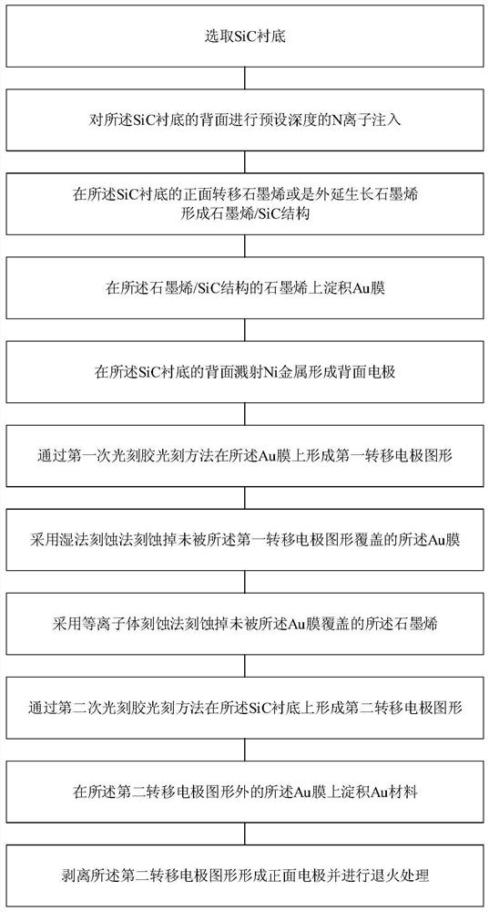
[0051] In order to improve the diffusion and electromigration of the contact metal to the semiconductor under the condition of ultra-high power or irradiation environment without increasing the specific contact resistivity as much as possible, please refer to figure 1 , Figure 2a ~ Figure 2h , figure 1 It is a schematic flow chart of a SiC-based ohmic contact preparation method using graphene as a diffusion barrier layer provided by an embodiment of the present invention, Figure 2a ~ Figure 2h It is a schematic structural diagram of a SiC-based ohmic contact preparation method using graphene as a diffusion barrier provided by an embodiment of the present invention. This embodiment provides a SiC-based ohmic contact preparation method using graphene as a diffusion barrier layer. The SiC-based ohmic contact preparation method using graphene as a diffusion barrier layer includes the following steps:

[0052] Step 1. Select a SiC substrate.

[0053] Specifically, the SiC subs...


PUM


Abstract

The invention discloses a SiC-based ohmic contact preparation method using graphene as a diffusion barrier layer, comprising: selecting a SiC substrate; performing N ion implantation at a preset depth on the back of the SiC substrate; Graphene / SiC structure; Au film is deposited on the graphene of Graphene / SiC structure; The back electrode is formed on the back side of SiC substrate; By photolithography, the first transfer electrode pattern is formed on the Au film; Au film covered by the first transfer electrode pattern; etching away the graphene not covered by the Au film; forming a second transfer electrode pattern on the SiC substrate by photolithography; on the Au film outside the second transfer electrode pattern depositing Au material; peeling off the second transfer electrode pattern to form the front electrode. The method of the invention is a feasible preparation scheme, and improves the problems of contact resistance diffusion and electromigration, improves the stability and service life of power devices, and the proposal of the new structure brings inspiration to the research of ohmic contact technology.

Description

technical field [0001] The invention belongs to the technical field of SiC-based ohmic contacts, and in particular relates to a method for preparing SiC-based ohmic contacts using graphene as a diffusion barrier layer. Background technique [0002] Due to its excellent characteristics such as wide bandgap, high thermal conductivity, and high breakdown electric field, SiC materials have irreplaceable advantages in extreme working conditions such as high temperature, high power, and irradiation, and have attracted much attention in various application fields. [0003] At present, the ever-shrinking device feature size puts forward higher requirements for ohmic contacts. The current density at the contact is doubled through the reduction of the metal contact window ratio, and the diffusion or electromigration of the contact metal to the semiconductor is a serious problem. When diffusion occurs in shallow junctions, it is easy to cause leakage current and short circuit, increase...

Claims


Application Information

Patent Timeline
Patent Type & Authority Patents(China)
IPC IPC(8): H01L29/45H01L29/16
CPCH01L29/45H01L29/1608
Inventor 胡彦飞纪宇婷郭辉梁佳博何艳静袁昊王雨田
Owner XIDIAN UNIV
Learn More