
Wafer mirror surface chamfering method, wafer manufacturing method, and wafer

A wafer and chamfering technology, applied in manufacturing tools, semiconductor/solid-state device manufacturing, machine tools suitable for grinding workpiece edges, etc., can solve problems such as dusting, and achieve the effect of suppressing edges

Pending Publication Date: 2021-01-12
SUMCO CORP
View PDF10 Cites 1 Cited by
  • Summary
  • Abstract
  • Description
  • Claims
  • Application Information

AI Technical Summary

Problems solved by technology

[0005] However, in the wafer whose mirror surface was chamfered by the method of Patent Document 1, it was found that in the process after the final cleaning process of the wafer, the wafer chuck and the groove in the wafer container came into contact with the wafer, and thus, there was a possibility of dust generation.
In addition, careful observation of the surface of the mirror-chamfered wafer reveals that corners are formed at the boundary between the main surface of the wafer and the chamfered surface, which may cause dust generation.

Method used


Image

  • Wafer mirror surface chamfering method, wafer manufacturing method, and wafer
  • Wafer mirror surface chamfering method, wafer manufacturing method, and wafer
  • Wafer mirror surface chamfering method, wafer manufacturing method, and wafer

Examples


Embodiment

[0054] (Invention Example 1)

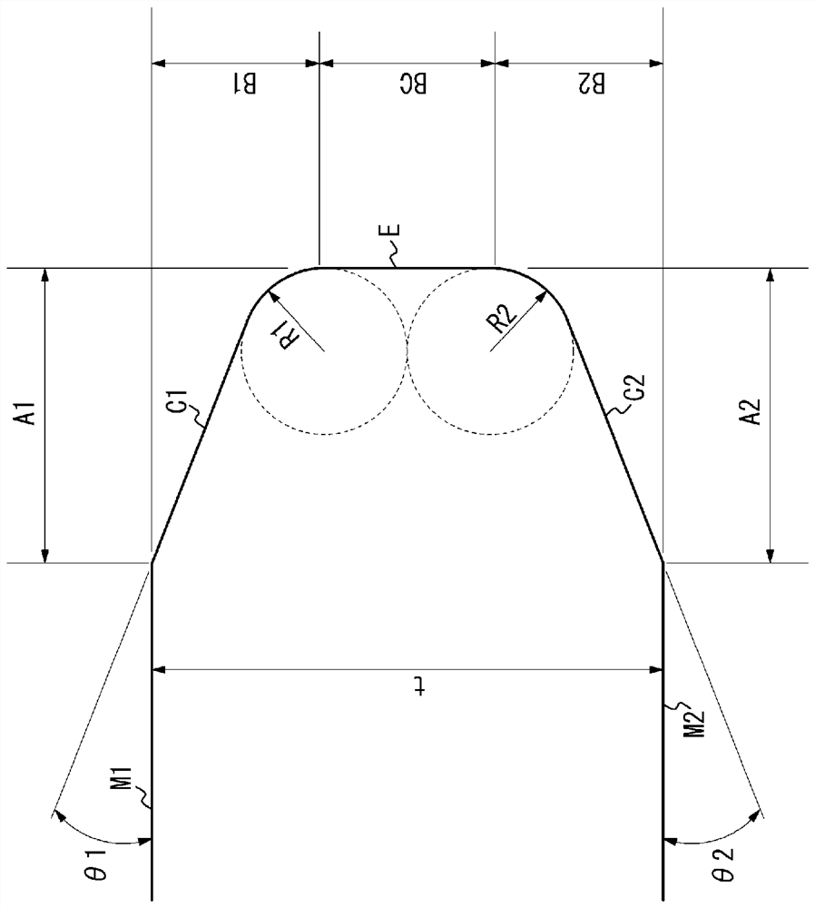
[0055] For a silicon wafer cut from a single crystal silicon ingot: 300 mm in diameter, chamfering, polishing, etching, and double-sided grinding were performed in this order to obtain 5 wafers with figure 1 A silicon wafer of the shape shown. Here, in the chamfering of the wafer, the target values ​​of θ1 and θ2 were set to 22° by a chamfering processing apparatus using a #2000 resin grindstone. Also, t=776 μm, A1=240 μm, A2=240 μm, B1=213 μm, B2=213 μm, BC=350 μm, R1=230 μm, R2=230 μm.

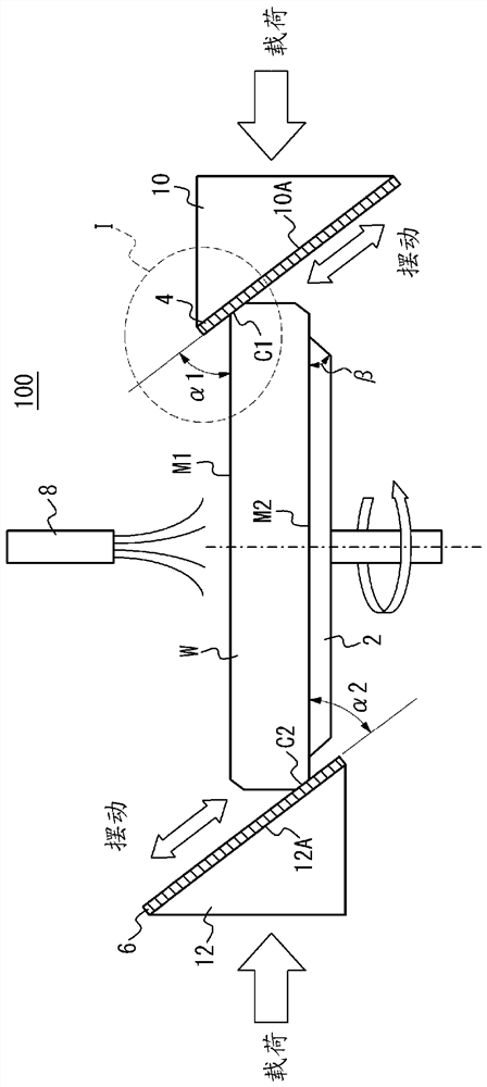
[0056] Next, use Figure 2A The shown mirror chamfering apparatus performs mirror chamfering on each silicon wafer under the following conditions.

[0057] α1, α2: 22°

[0058] β: 20°

[0059] Types of polishing pads 1 and 2: Polyurethane non-woven fabric

[0060] Compression rate of the first and second polishing pads: 5%

[0061] The thickness of the first and second polishing pads: 1.5mm

[0062] Swing speed of the 1st and 2nd polishing pad installat...


PUM


Abstract

Provided is a wafer mirror surface chamfering method by which corner burrs at the boundaries between main surfaces and chamfered surfaces of the wafer can be reduced. The present invention is a wafermirror surface chamfering method by which chamfered surfaces of a wafer (W) are mirror-polished using polishing pads (4, 6), the method being characterized in that respective angles ([alpha]1, [alpha]2) between main surfaces of polishing pads (4, 6) and main surfaces of a wafer (W) are set to at most a target value of a chamfering angle at the time of chamfering.

Description

technical field [0001] The invention relates to a mirror chamfering method of a wafer, a manufacturing method of the wafer and the wafer. Background technique [0002] Semiconductor elements are manufactured by performing chamfering, polishing, etching, double-side grinding, mirror chamfering, finish grinding, etc. on a wafer cut out from a single crystal ingot, and then forming an electrical circuit on the main surface of the wafer through an element process. Here, "chamfering" refers to the process of forming a chamfered surface on the periphery of the wafer using a grindstone for chamfering, etc., and "mirror surface chamfering" refers to mirror-finishing the chamfered surface formed by chamfering using a polishing pad. Grinding treatment. [0003] In Patent Document 1, mirror chamfering is performed on a chamfered wafer by the following method. That is, with respect to the chamfering surface of the wafer that is chamfered so that the angle formed by the main surface of...

Claims


Application Information

Patent Timeline
IPC IPC(8): B24B9/00H01L21/304
CPCB24B9/065B24B37/20H01L21/304C30B33/00B24B37/08H01L21/02021H01L21/02013H01L21/02024
Inventor 山下健儿
Owner SUMCO CORP
Learn More