A structure and design method for reducing mini LED mixed light area
A design method and area technology, applied in geometric CAD, semiconductor devices, electrical components, etc., can solve the problem of slight halo, and achieve the effect of avoiding halo, reducing area, and reducing light mixing.
- Summary
- Abstract
- Description
- Claims
- Application Information
AI Technical Summary
Problems solved by technology
Method used
Image
Examples
Embodiment Construction
[0022] The technical solution of the present invention will be clearly and completely described below in conjunction with the embodiments. Obviously, the described embodiments are only some embodiments of the present invention, rather than all embodiments. Based on the embodiments of the present invention, all other embodiments obtained by persons of ordinary skill in the art without creative efforts fall within the protection scope of the present invention.
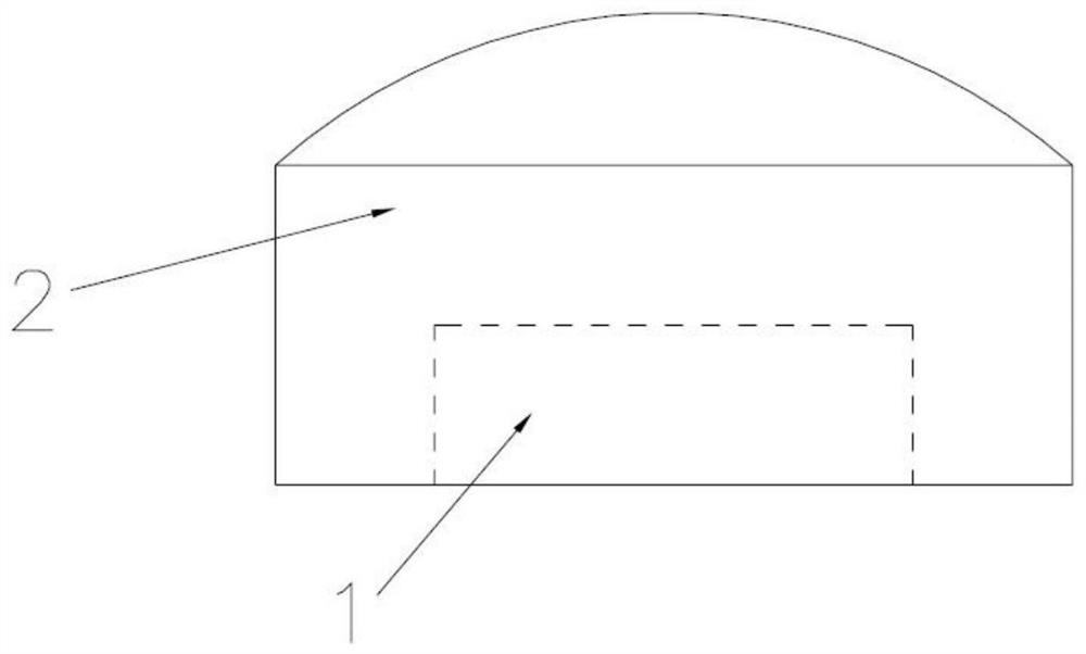
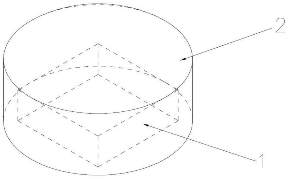
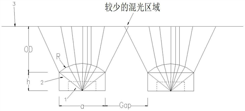
[0023] see Figure 1-4 As shown, a structure to reduce the mixed light area of Mini LED includes chip 1, which is encapsulated by convex sealant 2; convex sealant 2 is provided with an arc-shaped convex cup; the light generated by chip 1 passes through the convex The sealant 2 is irradiated on the diffusion plate or the diffusion film 3 with the same effect;
[0024] A design method for reducing the structure of the Mini LED mixed light area. By controlling the shape of the chip colloidal package, the surface of the c...
PUM
 Abstract
Description
Claims
Application Information


