

A high-precision stepped crimping hole processing method
A processing method and technology of crimping holes, which are applied to the formation of electrical connections of printed components, reduction of greenhouse gases, printed circuits, etc., can solve problems such as local open circuits, extremely poor board thickness, etc., to improve accuracy, reduce positioning point deviation, The effect of avoiding wasted space
- Summary
- Abstract
- Description
- Claims
- Application Information
AI Technical Summary
Problems solved by technology
Method used
Image

Examples
Embodiment Construction
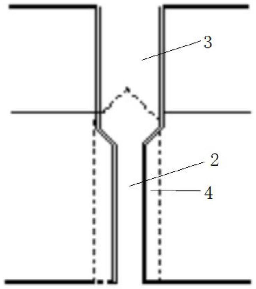
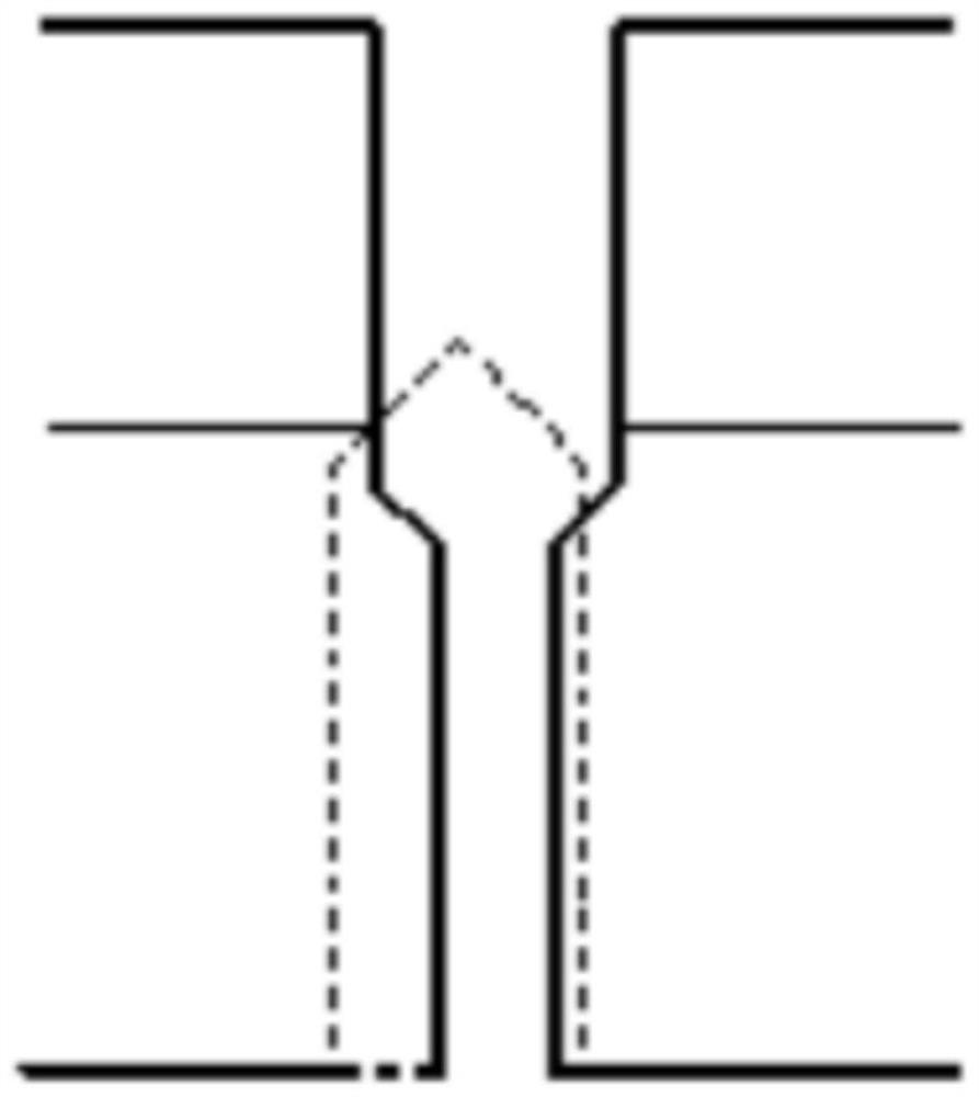
[0032] The drilling process of the present invention is as follows:
[0033] "Xray punching - measurement of expansion and contraction - pin positioning - mechanical drilling through holes - controlled depth drilling - sinking copper - electroplating - testing electroplating PIN hole size - high precision size pin nails - back drilling".
[0034] The specific control is as follows: set the thickness of the plate as H, the diameter of the depth control drill as R, and the diameter of the back drill as R 1 ; The diameter of the small hole is r; the deviation of the back-drilling accuracy is σ 1 , the deviation between the wall of the back-drilled hole and the wall of the controlled-depth drilled hole (without copper) is σ 2 ; The copper thickness of the plated hole is b. The diameter of the first pin is d 1 ; The diameter of the second pin is d 2 .
[0035] Main control requirements:
[0036] (1)d 2 = d 1 -2b, the thickness of b is generally 20-25μm.
[0037] (2) The di...
PUM
 Abstract
Description
Claims
Application Information