Cleaning device for semiconductor preparation

A cleaning device and a technology for semiconductors, which are used in the manufacture of semiconductor/solid-state devices, cleaning methods using liquids, and solid separation, etc., can solve the problems of time-consuming and laborious semiconductor wafers, unfavorable semiconductor cleaning, and dead corners of semiconductor cleaning, and achieve good fixing effect. The effect of improving convenience and ensuring service life

Inactive Publication Date: 2021-03-09
广州夕千科技有限公司
View PDF0 Cites 1 Cited by
  • Summary
  • Abstract
  • Description
  • Claims
  • Application Information

AI Technical Summary

Problems solved by technology

[0002] The cleaning of semiconductor chips is a very delicate work, and the requirements for the cleaning environment of semiconductor chips are relatively strict. The existing semiconductor cleaning device generally cleans the semiconductor by simply fixing it; it is difficult for the existing semiconductor cleaning device to clean the semiconductor surface in an all-round and uniform manner during the cleaning process of the semiconductor, and it is easy to produce a dead angle for cleaning the semiconductor. , which is not conducive to better cleaning of semiconductors, and is not conducive to improving the convenience of use

Method used


Image

  • Cleaning device for semiconductor preparation
  • Cleaning device for semiconductor preparation
  • Cleaning device for semiconductor preparation

Examples


Embodiment Construction

[0050] The following will clearly and completely describe the technical solutions in the embodiments of the present invention with reference to the accompanying drawings in the embodiments of the present invention. Obviously, the described embodiments are only some, not all, embodiments of the present invention. Based on the embodiments of the present invention, all other embodiments obtained by persons of ordinary skill in the art without making creative efforts belong to the protection scope of the present invention.

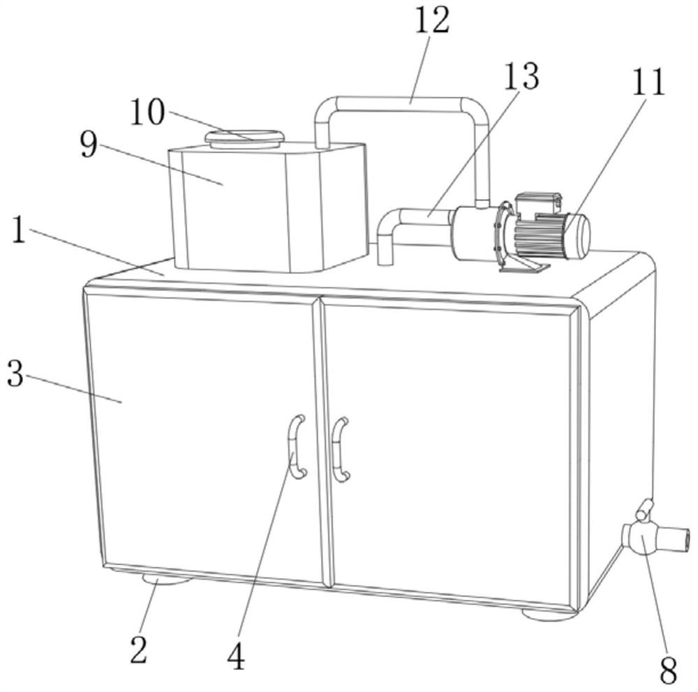
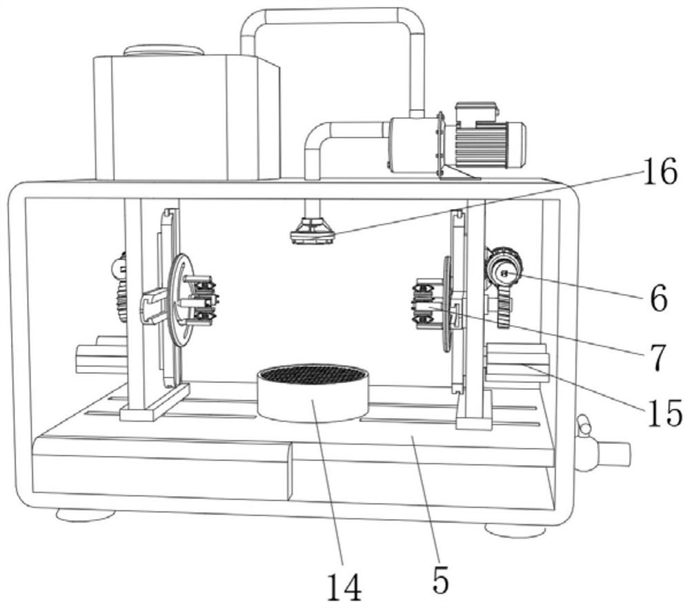
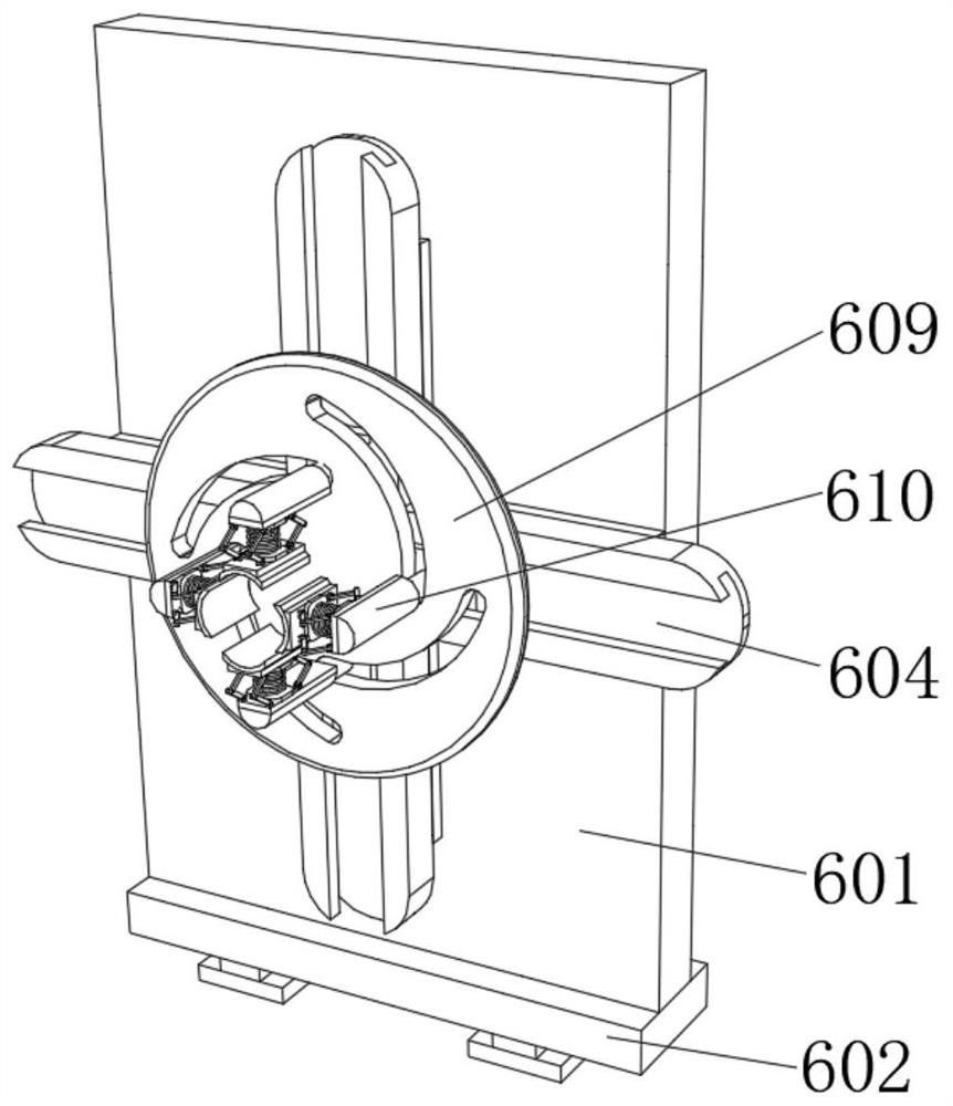
[0051] see Figure 1-5 , the present invention provides a technical solution: a cleaning device for semiconductor preparation, including a cleaning box 1, the four corners of the lower surface of the cleaning box 1 are fixedly connected with a fixed base 2, the front of the cleaning box 1 is provided with a door panel 3, the door panel 3 The front is fixedly connected with an operating handle 4, and the inner bottom of the cleaning box 1 is fixedly connected w...


PUM


Abstract

The invention relates to the technical field of semiconductors, and discloses a cleaning device for semiconductor preparation. The cleaning device comprises a cleaning box, wherein fixed bases are fixedly connected to the four corners of the lower surface of the cleaning box; a door plate is arranged on the front face of the cleaning box; an operation handle is fixedly connected to the front faceof the door plate; a fixing plate is fixedly connected to the inner bottom of the cleaning box; movable rotating devices are arranged on the left side and the right side of the upper surface of the fixing plate correspondingly; and clamping devices are arranged on the inner sides of the movable rotating devices. According to the cleaning device for semiconductor preparation, a driving motor drivesa rotating disc to drive a sliding column to move inwards to move a semiconductor to be clamped and fixed, so that a better fixing effect is achieved on the semiconductor, the surface of the semiconductor can be better and uniformly cleaned in all directions, cleaning dead corners of the semiconductor are effectively reduced, the semiconductor can be better cleaned, the cleaning effect of the semiconductor is improved, and the use convenience is improved.

Description

technical field [0001] The invention relates to the technical field of semiconductors, in particular to a cleaning device for semiconductor preparation. Background technique [0002] The cleaning of semiconductor chips is a very delicate work, and the requirements for the cleaning environment of semiconductor chips are relatively strict. The existing semiconductor cleaning device generally cleans the semiconductor by simply fixing it; it is difficult for the existing semiconductor cleaning device to clean the semiconductor surface in an all-round and uniform manner during the cleaning process of the semiconductor, and it is easy to produce a dead angle for cleaning the semiconductor. , It is not conducive to better cleaning of semiconductors, and it is not conducive to the improvement of convenience. Contents of the invention [0003] (1) Solved technical problems [0004] Aiming at the deficiencies of the prior art, the present invention provides a cleaning device for s...

Claims


Application Information

Patent Timeline
Patent Type & Authority Applications(China)
IPC IPC(8): B08B3/02B08B13/00B03C3/017H01L21/67H01L21/687
CPCB03C3/017B08B3/02B08B13/00H01L21/67051H01L21/687
Inventor 林淑毜
Owner 广州夕千科技有限公司
Why Eureka
Try Eureka