Preparation method of display panel, display panel and display device
A display panel and display area technology, applied in identification devices, semiconductor/solid-state device manufacturing, data processing input/output process, etc., can solve problems such as film layer separation, poor touch, peeling, etc., to eliminate bubbling, Effects that guarantee good performance
- Summary
- Abstract
- Description
- Claims
- Application Information
AI Technical Summary
Problems solved by technology
Method used
Image
Examples
Embodiment Construction
[0068] Example embodiments will now be described more fully with reference to the accompanying drawings. Example embodiments may, however, be embodied in many forms and should not be construed as limited to the embodiments set forth herein; rather, these embodiments are provided so that this disclosure will be thorough and complete, and will fully convey the concept of example embodiments to those skilled in the art. The same reference numerals in the drawings denote the same or similar structures, and thus their detailed descriptions will be omitted.
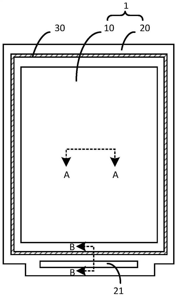
[0069] refer to figure 1 , is a top view of a display panel with an FMLOC structure, and the display panel includes a centrally located display area 10 and a peripheral area 20 surrounding the display area.
[0070] Part of the display area is provided with a pixel circuit, an OLED light-emitting device is provided above the pixel circuit, a packaging layer is provided above the OLED light-emitting device, and a touch functio...
PUM
 Abstract
Description
Claims
Application Information


