A processing method for high aspect ratio structures of hard and brittle materials and its application in the preparation of optical micro-nano structures
A high aspect ratio structure and processing method technology, applied in metal processing equipment, welding equipment, manufacturing tools, etc., can solve problems such as hindering etching, and achieve high smoothness, material removal, and high precision.
- Summary
- Abstract
- Description
- Claims
- Application Information
AI Technical Summary
Problems solved by technology
Method used
Image
Examples
Embodiment 1
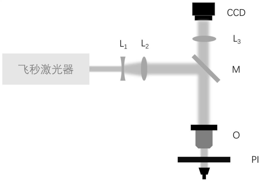
[0032] Depend on figure 1 As shown, the 343nm femtosecond laser emitted by the laser passes through the quartz first concave lens L sequentially 1 and the second convex lens L 2 Beam expansion; then the beam reaches the objective lens O through the total reflection mirror M; in addition, the mercury lamp light source passes through the processed sample, the focusing ring objective lens O, the total reflection mirror M, and then passes through the third convex lens L 3 to the image sensor CCD.
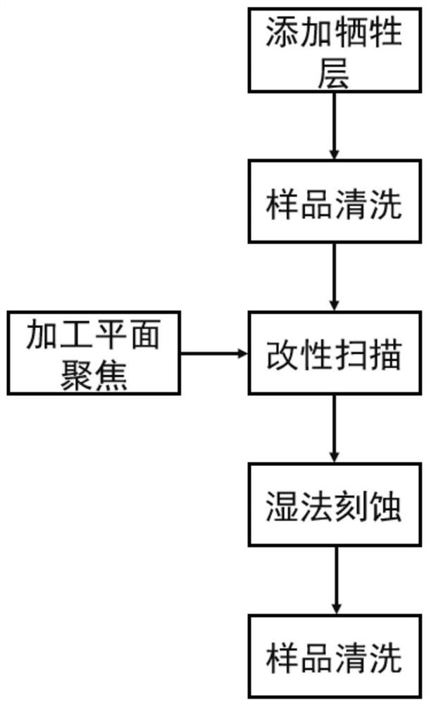
[0033] A processing method for a high aspect ratio structure of a hard and brittle material, the specific steps are as follows:
[0034] Step 1: Preparation of samples to be processed;
[0035]First, silicon dioxide was sputtered on the surface of the sapphire sample by magnetron sputtering at a substrate temperature of 250°C, a radio frequency power of 2KW, and a sputtering pressure of 0.5Pa. The thickness of the silicon dioxide was 3m, and the thickness of the sapphire substrate wa...
Embodiment 2
[0043] Subwavelength antireflection structures were fabricated on sapphire surfaces by etching-assisted femtosecond laser modification with a sacrificial layer.
[0044] The cleaned sapphire sample was dry-etched using an ICP etching system (ICP-100A, TAILONG ELECTRONICS). For the sapphire material, the etching gas was a mixture of chlorine and boron trichloride. The parameters of ICP etching are set as follows: the upper electrode power of the ICP etching system is 600W, and the lower electrode power is 300W. The etching gas is a mixed gas of chlorine gas and boron trichloride, and the gas flow rates are respectively 20 sccm of chlorine gas and 30 sccm of boron trichloride. After dry etching for 50 minutes, a pyramid-like structure with good surface quality is formed, which has a sub-wavelength anti-reflection effect, and realizes the preparation of a sub-wavelength anti-reflection structure on the surface of sapphire.
[0045] Depend on Figure 5 It can be seen that the su...
PUM
| Property | Measurement | Unit |
|---|---|---|
| thickness | aaaaa | aaaaa |
| thickness | aaaaa | aaaaa |
Abstract
Description
Claims
Application Information


