Fingerprint detection device

A detection device, fingerprint technology, applied in the direction of acquiring/organizing fingerprints/palmprints, instruments, electrical components, etc., can solve the problem of reducing the effective sensing area of ​​the sensing electrode, melting or vaporizing the surrounding materials of the shunt structure, and capacitive fingerprint identification device Damage and other issues

Pending Publication Date: 2021-03-30
SUPERC TOUCH CORP
View PDF0 Cites 0 Cited by
  • Summary
  • Abstract
  • Description
  • Claims
  • Application Information

AI Technical Summary

Problems solved by technology

[0004] Although it has been proposed to use a shunt structure to strengthen electrostatic protection, electrostatic discharge often generates extremely high temperatures in the shunt structure instantly, causing the shunt structure itself or its surrounding materials to melt or vaporize, or even burst, and eventually cause irreversible damage t

Method used


Image

  • Fingerprint detection device
  • Fingerprint detection device
  • Fingerprint detection device

Examples


Embodiment Construction

[0083] Various embodiments of the invention are provided below. These examples are used to illustrate the technical content of the present invention, but not to limit the scope of rights of the present invention. A feature of one embodiment can be applied to other embodiments through appropriate modification, replacement, combination, and separation.

[0084] It should be noted that in this article, unless otherwise specified, possessing "a" component is not limited to possessing a single such component, but may possess one or more such components.

[0085] In addition, in this article, unless otherwise specified, ordinal numbers such as "first" and "second" are only used to distinguish multiple components with the same name, and do not indicate that there is a hierarchy, level, or execution order between them , or process sequence. A "first" component and a "second" component may appear together in the same component, or separately in different components. The presence of ...


PUM

PropertyMeasurementUnit
Thermal conductivityaaaaaaaaaa

Abstract

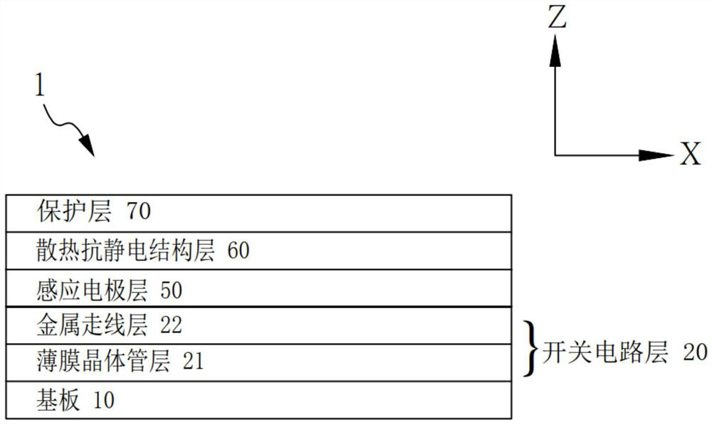
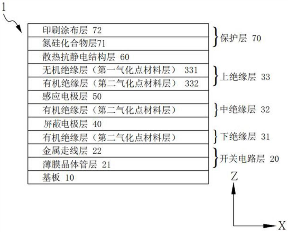
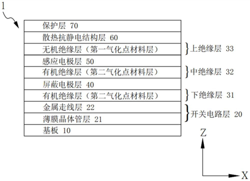
The invention provides a fingerprint detection device. The fingerprint detection device comprises a substrate, a switch circuit layer, an induction electrode layer, a heat dissipation antistatic structure layer and a protection layer. The switch circuit layer is arranged on the substrate and comprises a plurality of transistor switches, a plurality of data lines and a plurality of control lines. The induction electrode layer is arranged on the switch circuit layer and comprises a plurality of induction electrodes. The heat dissipation antistatic structure layer is arranged on the induction electrode layer. The heat dissipation antistatic structure layer comprises a conductive grid and a plurality of shunt radiators. The conductive grid is provided with a plurality of meshes and is configured to conduct charges. The shunt radiators are adjacent to the conductive grid and correspond to the induction electrodes. The shunt radiators are electrically insulated from each other, are electrically insulated from the conductive grid, and are electrically insulated from the induction electrodes. The protection layer is arranged on the heat dissipation antistatic structure layer.

Description

technical field [0001] The present invention relates to a fingerprint detection device, in particular to a fingerprint detection device with an antistatic structure, and more particularly to a fingerprint detection device with a heat dissipation and antistatic structure. Background technique [0002] Now, with the rise of e-commerce, the development of remote payment is also advancing by leaps and bounds. In order to cooperate with remote payment, the demand for biometric identification is rapidly expanding. Among them, based on the requirements of efficiency, safety, and non-invasiveness, fingerprint recognition has become the first choice for biometrics, especially capacitive fingerprint detection, which stands out under the comprehensive consideration of device size, manufacturing cost, power saving, reliability, and anti-counterfeiting. [0003] However, the severe problem faced by the capacitive fingerprint recognition device is its low electrostatic tolerance. This i...

Claims


Application Information

Patent Timeline
IPC IPC(8): G06K9/00H01L23/60
CPCH01L23/60G06V40/1306
Inventor 李祥宇金上林丙村杜佳动
Owner SUPERC TOUCH CORP
Why Eureka
Try Eureka