
Patsnap Eureka
For R&D, Patsnap Eureka makes reading and utilizing patents & technical documents easy.
Patsnap Eureka AIR
Designed for self-driven R&D workflows. Generate viable solutions, solve complex R&D challenges, empower your innovation with AI.

Patsnap Eureka Materials
Designed for material experts only. Revolutionize your material R&D, from search, analyze, to developing new materials.

TechResearch
Generate reliable direction feasibility study reports for your R&D in just a few steps.

TechSeek
Discover and master advanced knowledge NOW. Basics, ideas, possibilities, all at once.

TechMind
As an expert in R&D Theories, TechMind can generates customized viable solutions instantly.

TechRisk
Analyze your overall solution with one click, know your potential R&D risks in advance.

TechMonitor
Get weekly tech updates, stay abreast of the latest tech innovations and key insights.
Liquid crystal micro-lens array imaging device, driving method and electronic equipment
A liquid crystal microlens and lens array technology, applied in the field of imaging, can solve the problem of reducing the dynamic range of image sensors and achieve the effect of reducing light efficiency
- Summary
- Abstract
- Description
- Claims
- Application Information
AI Technical Summary
Problems solved by technology
Method used
Image

Examples
Embodiment 1
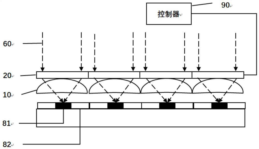
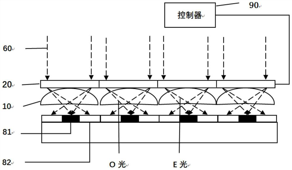
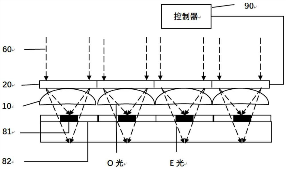
[0026] see Figure 1 to Figure 4 , the embodiment of the present invention discloses a liquid crystal microlens array imaging device, including: a first lens array 10, a second lens array 20, an image sensor, a photosensitive area 81 arranged on the image sensor, and a controller 90; the first The second lens array 20 is located above the first lens array 10, and changes the refractive index according to the driving voltage. The second lens array here can be a liquid microlens array or a liquid crystal microlens array; the first lens array 10 is located on the Between the photosensitive area 81 and the second lens array 20, it is used to focus the incident light 60 on the photosensitive area 81 after refracting the second lens array 20; The receiving amount adjusts the driving voltage of the second lens array 20 . Each image sensor is provided with a photosensitive area 81 . When the cumulative light receiving amount of the photosensitive area 81 is relatively large, the dri...
Embodiment 2
[0061] see Figure 5 , the present invention also discloses a driving method based on the aforementioned liquid crystal microlens array imaging device, the driving method comprising:
[0062] S10. Comparing the cumulative light-receiving amount of the photosensitive area with a preset value;
[0063] S20. Sending a driving voltage command according to the comparison result. The driving voltage command includes one of the first driving voltage command, the second driving voltage command and the third driving voltage command.
[0064] S30 , outputting a driving voltage according to the driving voltage command to drive the second lens array 20 to work. Therefore, the automatic adjustment of the refractive index of the second lens array 20 is realized, and the light efficiency of the image sensor is improved while the dynamic range of the image sensor is improved.
[0065] Wherein, S30, outputting a driving voltage according to the driving voltage instruction to drive the second ...
Embodiment 3
[0074] The present invention also discloses an electronic device, including a liquid crystal microlens array imaging device, the liquid crystal microlens array imaging device is the liquid crystal microlens array imaging device described in any one of the first aspect and / or adopts any one of the second aspect One of the drive methods described. The liquid crystal microlens array imaging device adjusts the driving voltage of the second lens array 20 to adjust the driving voltage of the second lens array 20 through the cumulative light receiving amount of the photosensitive area 81 when the cumulative light receiving amount of the photosensitive area 81 is relatively large. The refractive index makes the focal point of e light deviate from the photosensitive area 81, thereby reducing the light efficiency of the image sensor; when the cumulative light receiving amount of the photosensitive area 81 is small, no driving voltage is applied to the second lens array 20, and the light ...
PUM
 Abstract
Description
Claims
Application Information
 - R&D Engineer
- R&D Manager
- IP Professional
- Industry Leading Data Capabilities
- Powerful AI technology
- Patent DNA Extraction
Browse by: Latest US Patents, China's latest patents, Technical Efficacy Thesaurus, Application Domain, Technology Topic, Popular Technical Reports.
© 2024 PatSnap. All rights reserved.Legal|Privacy policy|Modern Slavery Act Transparency Statement|Sitemap|About US| Contact US: help@patsnap.com