
SMT printing process burst buckle jig

A printing process and fixture technology, which is applied in the direction of assembling printed circuits with electrical components and forming conductive patterns, etc., which can solve problems such as poor printing, waste of cost, and low work efficiency

Pending Publication Date: 2021-04-20
苏州市凯思泰克自动化设备有限公司
View PDF0 Cites 0 Cited by
  • Summary
  • Abstract
  • Description
  • Claims
  • Application Information

AI Technical Summary

Problems solved by technology

[0003] 1. Carrier-free printing is generally only suitable for thicker PCB boards, and it cannot be printed directly for thinner PCB boards;
[0004] 2. Carrier printing is widely used, but for thinner PCB boards, it is necessary to use a pressure plate, or use adhesive tape to fix the PCB, otherwise it will cause the PCB to warp, and eventually cause poor printing and waste costs; and The sticking tape before printing and the tearing tape at the back end need to be completed by the staff, which will not only cause cost waste, low work efficiency, error-prone and other problems, but also cannot realize the fully automatic operation mode

Method used


Image

  • SMT printing process burst buckle jig
  • SMT printing process burst buckle jig
  • SMT printing process burst buckle jig

Examples


Embodiment Construction

[0023]In order to make the objects, technical solutions and advantages of the present invention, the invention will be further described in detail below with reference to the embodiments. The specific embodiments described herein are for explaining the invention and is not intended to limit the invention.

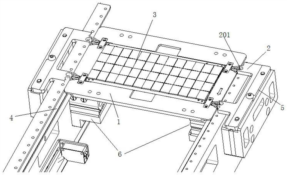
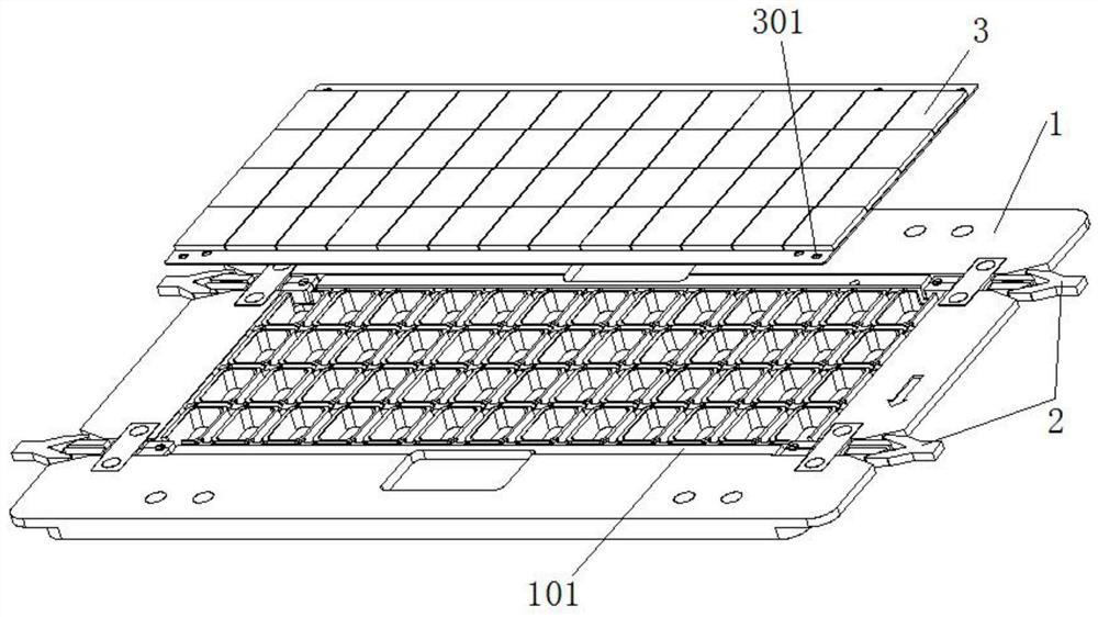
[0024]Such asFigure 1 - Figure 3As shown, the SMT printing process buckle assignment of the present embodiment includes a trigger body 1 disposed on the frame 4, and the fixture body 1 is a recess 101 for placing the PCB plate 3, the PCB plate. The four corners of the 3 have a positioning aperture 301, and a set of positioning mechanisms for tightening the positioning hole 301 on the PCB plate is provided on both ends of the groove 101, each set of positioning mechanisms including two. Symmetric distribution buckle mechanism.

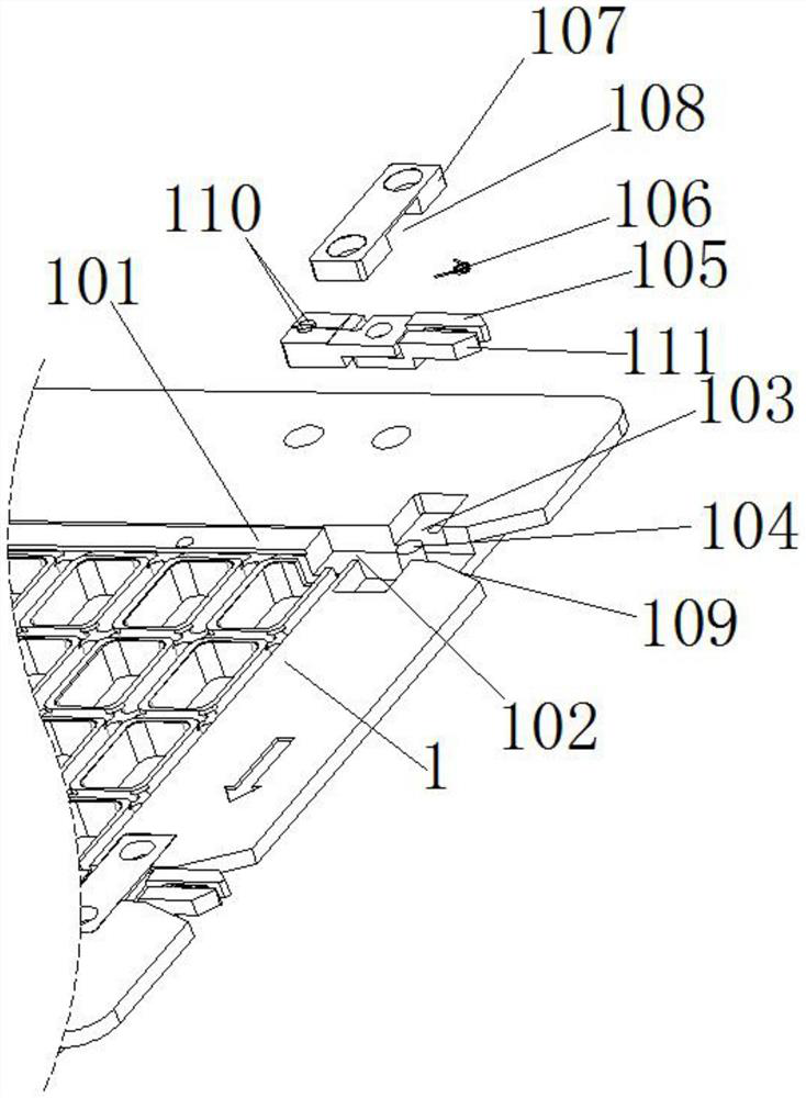
[0025]Specifically, such asfigure 2 ,image 3 As shown, the bursting mechanism includes a first mounting groove 102, a second mounting groove 103, two active jaw...


PUM


Abstract

The invention discloses an SMT printing process burst buckle jig which comprises a jig body arranged on a rack. A groove used for containing a PCB is formed in the jig body, positioning holes are formed in the four corners of the PCB, and the positions, at the two ends of the groove, of the jig body are each provided with a set of positioning mechanisms used for tensioning the positioning holes in the PCB. And each set of positioning mechanisms comprises two symmetrically distributed burst buckle mechanisms. Compared with the prior art, by using the jig of the invention, two burst buckle mechanisms of each set of positioning mechanisms can be independently exploded, the positioning holes in the PCB can be independently expanded, the jig can be suitable for the PCB with the thickness of 0.3 mm-1.2 mm, the utilization rate is greatly increased, and the application range is expanded.

Description

Technical field[0001]The present invention relates to the technical field of circuit board printing fixtures, in particular a SMT printing process buckle.Background technique[0002]SMT printing in the prior art is divided into two, no load printing and printing;[0003]1. No load printing is generally only suitable for a thickness of PCB plates, which cannot be directly printed for a PCB plate having a thin thickness;[0004]2. The carrier printing is widely used, but for thinner PCB board factors, the pressure plate must be used, or the PCB is fixed using the rubber band, otherwise the PCB will be made up, and it will eventually cause printing, waste, cost; The tape and back tape before printing require staff to complete, not only cause cost waste, low work efficiency, easy error, etc., but also unable to achieve fully automated operation mode.[0005]Therefore, it is necessary to improve the SMT printing fixture in the prior art.Inventive content[0006]It is an object of the present inven...

Claims


Application Information

Patent Timeline
IPC IPC(8): H05K3/12H05K3/34
Inventor 陈兵
Owner 苏州市凯思泰克自动化设备有限公司
Learn More