Redistribution layer structure and semiconductor package
A rewiring layer, semiconductor technology, applied in the direction of semiconductor devices, semiconductor/solid-state device components, electric solid-state devices, etc., can solve problems such as increasing production costs, and achieve the effect of reducing the number and reducing production costs
- Summary
- Abstract
- Description
- Claims
- Application Information
AI Technical Summary
Problems solved by technology
Method used
Image

Examples
Embodiment Construction
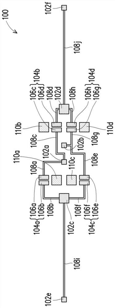
[0045] figure 1 It is a top view of a redistribution layer structure according to an embodiment of the present invention.
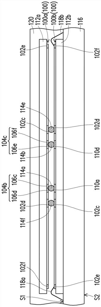
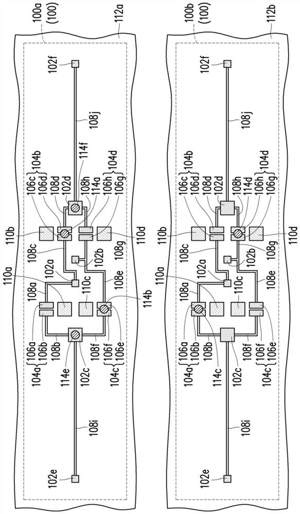
[0046] Please refer to figure 1 The redistribution layer structure 100 includes a pad 102a, a pad 102b, a pad 102c, a pad 102d, a switch element 104a, a switch element 104b, a switch element 104c, and a switch element 104d. The redistribution layer structure 100 is, for example, a redistribution layer layout pattern.
[0047] The pad 102a, the pad 102b, the pad 102c and the pad 102d are separated from each other. In this embodiment, the pads 102a and 102b can be used as die pads, and the pads 102c and 102d can be used as solder pads, but the present invention does not take this as an example. limit. In addition, the pads 102a and 102b are, for example, located between the pads 102c and 102d, but the invention is not limited thereto. Those skilled in the art can adjust the arrangement of the pads 102a, 102b, 102c, and 102d according to product design....
PUM
 Abstract
Description
Claims
Application Information
 - R&D
- Intellectual Property
- Life Sciences
- Materials
- Tech Scout
- Unparalleled Data Quality
- Higher Quality Content
- 60% Fewer Hallucinations
Browse by: Latest US Patents, China's latest patents, Technical Efficacy Thesaurus, Application Domain, Technology Topic, Popular Technical Reports.
© 2025 PatSnap. All rights reserved.Legal|Privacy policy|Modern Slavery Act Transparency Statement|Sitemap|About US| Contact US: help@patsnap.com