Photoelectric conversion device

A photoelectric conversion device and photodiode technology, applied in photovoltaic power generation, circuits, electrical components, etc., can solve the problems that the electrical performance of image sensors needs to be improved

Pending Publication Date: 2021-06-01
尤小月
View PDF0 Cites 0 Cited by
  • Summary
  • Abstract
  • Description
  • Claims
  • Application Information

AI Technical Summary

Problems solved by technology

[0003] However, the electrical performance of existing image sensors still needs to be improved

Method used


Image

  • Photoelectric conversion device
  • Photoelectric conversion device
  • Photoelectric conversion device

Examples


Embodiment Construction

[0035] Embodiments of the present disclosure will be described with reference to the drawings. Hereinafter, parts corresponding to each other in the drawings will be denoted by the same reference numerals.

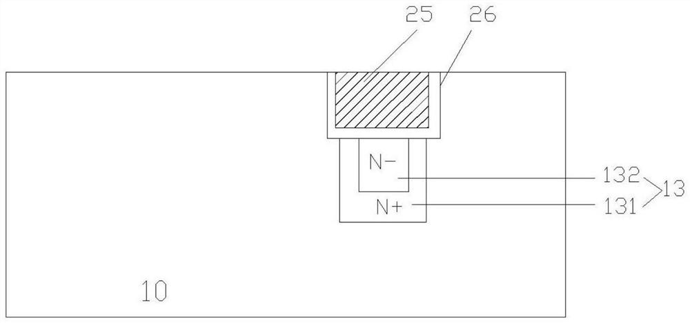
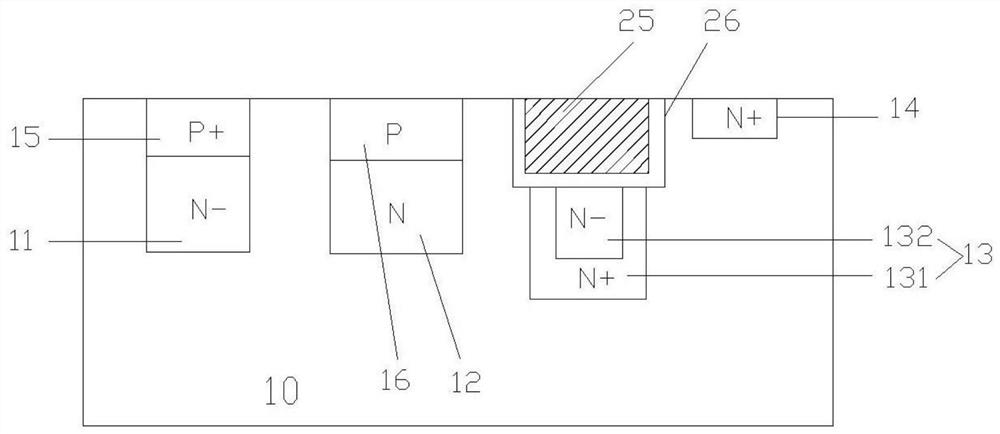
[0036] Figure 1 to Figure 4 is a schematic diagram of a method for forming a photoelectric conversion device in the present invention.

[0037] Such as figure 1 As shown, a P-type semiconductor substrate 10 is provided, and a trench is formed in the P-type semiconductor substrate 10 .

[0038] Such as figure 2 As shown, the P-type semiconductor substrate 10 at the bottom of the trench is N-type doped to form a suspended doped region 13, and the N-type doped is doped with impurities such as phosphorus; the suspended doped The region 13 includes an N+ type sub-suspension doped region 131 and an N-type sub-suspension doped region 132, the N+ type sub-suspension doped region 131 surrounds the N-type sub-suspension doped region 132; the N+ type sub-suspension doped region...


PUM


Abstract

The invention discloses a photoelectric conversion device, which includes a P-type semiconductor substrate, an N- type photodiode doped region, a P+ type hole accumulation region, an N type charge retention region, a P type charge blocking region, and a transmission gate electrode, a multiplication gate electrode and a reading gate electrode which arelocated above a gate insulating layer, a reset gate electrode structure, a suspension doped region including an N+ type sub-suspension doped region and an N- type sub-suspension doped region, and an N+ type reset drain region, wherein the N+ type sub suspension doped region surrounds the N- type sub suspension doped region, so that electric leakage from the N- type photodiode doped region to the N+ type reset drain region can be effectively avoided, and the electrical performance is improved.

Description

technical field [0001] The invention relates to the field of semiconductor manufacturing, in particular to a photoelectric conversion device and a forming method thereof. Background technique [0002] The principle of the photoelectric conversion device is that photons transfer energy to electrons to make them move to form an electric current, which can be used in solid-state imaging devices. The scene to be photographed is imaged on the photoelectric target through the optical system of the camera. Because the brightness of each point of the light image is different, the intensity of light received by each unit of the target surface is different, resulting in different resistance values ​​of each unit of the target surface. The resistance value of the target unit corresponding to the brighter pixel is smaller, and the resistance value of the target unit corresponding to the darker pixel is larger, so that the different brightness of each pixel on an image appears as the dif...

Claims


Application Information

Patent Timeline
IPC IPC(8): H01L31/0352H01L31/0224
CPCH01L31/035272H01L31/03529H01L31/035281H01L31/022408Y02E10/50
Inventor 尤小月
Owner 尤小月
Why Eureka
Try Eureka