Image sensor and method of forming the same

A technology of image sensor and transmission grid, which is applied in the direction of radiation control devices, etc., can solve the problems that the performance of CMOS image sensors needs to be improved, and achieve the effect of suppressing leakage

Active Publication Date: 2021-08-31
淮安西德工业设计有限公司
View PDF5 Cites 0 Cited by
  • Summary
  • Abstract
  • Description
  • Claims
  • Application Information

AI Technical Summary

Problems solved by technology

[0004] However, the performance of existing CMOS image sensors needs to be improved

Method used


Image

  • Image sensor and method of forming the same
  • Image sensor and method of forming the same
  • Image sensor and method of forming the same

Examples


Embodiment Construction

[0023] As mentioned in the background, semiconductor devices formed in the prior art have poor performance.

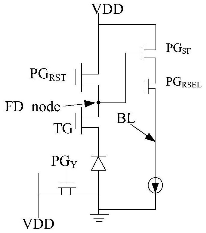
[0024] An image sensor pixel circuit, please refer to figure 1 , including: a photodiode; a transfer transistor TG, the source of the transfer transistor TG is connected to the photodiode; a floating diffusion FD node, the drain of the floating diffusion FD node is connected to the transfer transistor TG ; reset transistor PG RST , the reset transistor PG RST The source of is connected to the floating diffusion point FD node, and the reset transistor PG RST The drain is connected to the power line VDD; the source follows the transistor PG SF , the source follower transistor PG SF The gate of is connected to the floating diffusion point FD node, and the source follows the transistor PG SF The drain of the power supply line VDD is connected; the selection transistor PG RSEL , the selection transistor PG RSEL The drain of the source follower transistor PG with the ...


PUM

PropertyMeasurementUnit
depthaaaaaaaaaa
depthaaaaaaaaaa

Abstract

An image sensor and a method of forming the same, the image sensor comprising: a semiconductor substrate; an overflow gate structure in the semiconductor substrate, the overflow gate structure having opposite first and second sides; an overflow drain region in the semiconductor substrate on the first side of the gate structure, the overflow drain region is suitable for electrically connecting power lines; a diode doped layer, the diode doped layer is located on the semiconductor substrate on the second side of the overflow gate structure In; an additional floating diffusion region located in the semiconductor substrate at the bottom of the overflow gate structure, the additional floating diffusion region and the diode doping layer are separated from each other and separated from the overflow drain region. The performance of the image sensor is improved.

Description

technical field [0001] The invention relates to the field of semiconductor manufacturing, in particular to an image sensor and a forming method thereof. Background technique [0002] An image sensor is a semiconductor device that converts light signals into electrical signals. [0003] Image sensors are classified into complementary metal oxide (CMOS) image sensors and charge coupled device (CCD) image sensors. CMOS image sensor has the advantages of simple process, easy integration of other devices, small size, light weight, low power consumption and low cost. Therefore, with the development of image sensing technology, CMOS image sensors are increasingly used in various electronic products instead of CCD image sensors. At present, CMOS image sensors have been widely used in still digital cameras, digital video cameras, medical imaging devices, and automotive imaging devices. [0004] However, the performance of existing CMOS image sensors needs to be improved. Content...

Claims


Application Information

Patent Timeline
Patent Type & Authority Patents(China)
IPC IPC(8): H01L27/146
Inventor 王阳阳夏春秋汤茂亮刘少东
Owner 淮安西德工业设计有限公司
Why Eureka
Try Eureka