Forming method of image sensor

A technology of image sensors and doped regions, which is applied in the direction of electric solid-state devices, semiconductor devices, electrical components, etc., can solve the problems that the electrical performance of image sensors needs to be improved, and achieve the effect of increasing the channel length and suppressing leakage

Pending Publication Date: 2021-04-09
尤小月
View PDF0 Cites 2 Cited by
  • Summary
  • Abstract
  • Description
  • Claims
  • Application Information

AI Technical Summary

Problems solved by technology

[0003] However, the electrical performance of existing image sensors still needs to be improved

Method used


Image

  • Forming method of image sensor
  • Forming method of image sensor
  • Forming method of image sensor

Examples


Embodiment Construction

[0023] As mentioned in the background, the performance of the image sensor formed by the prior art is relatively poor.

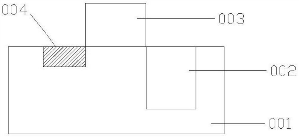
[0024] figure 1 It is a schematic diagram of a partial structure of an image sensor in the prior art, and the image sensor includes: a semiconductor substrate 001; an overflow gate structure 002 located on the semiconductor substrate 001; a diode located in the semiconductor substrate 001 on one side of the overflow gate structure 002 The doped region 003; the overflow drain region 004 located in the semiconductor substrate 001 on the other side of the overflow gate structure 002, and the overflow drain region 004 is electrically connected to the power line.

[0025] The overflow transistor PG Y The role includes: overflow transistor PG Y The drain of the VDD needs to be connected to the power supply line VDD at all times, and will overflow the transistor PG during the clearing sequence step Y Turn on to empty the charge in the photodiode.

[0026] In th...


PUM


Abstract

The invention discloses a forming method of an image sensor. The method comprises the steps that: a semiconductor substrate is provided; a gate trench is formed on the semiconductor substrate, an overflow gate insulating layer is formed at the bottom and on the side surface of the gate trench, an overflow gate electrode is formed on the overflow gate insulating layer, and an overflow gate structure is formed by the overflow gate insulating layer and the overflow gate electrode, wherein the overflow gate structure is provided with a first side surface and a second side surface opposite to the first side surface; a diode doped region is formed in the semiconductor substrate on the surface of the first side of the overflow gate structure; and an overflow drain region is formed in the semiconductor substrate on the surface of the second side of the overflow gate structure, wherein the overflow drain region is electrically connected with a power line, and the depth of the overflow gate structure is smaller than the depth of the diode doped region and larger than the depth of the overflow drain region. The performance of the image sensor is improved.

Description

technical field [0001] The invention relates to the field of semiconductor manufacturing, in particular to an image sensor and a forming method thereof. Background technique [0002] The image sensor uses the photoelectric conversion function of the photoelectric device to convert the light image on the photosensitive surface into an electrical signal proportional to the light image. Compared with photosensitive elements of "point" light sources such as photodiodes and phototransistors, the image sensor is a functional device that divides the light image on its light-receiving surface into many small units and converts it into usable electrical signals. Image sensors are divided into photoconductive camera tubes and solid-state image sensors. Compared with photoconductive camera tubes, solid-state image sensors have the characteristics of small size, light weight, high integration, high resolution, low power consumption, long life, and low price. Therefore, it has been wid...

Claims


Application Information

Patent Timeline
IPC IPC(8): H01L27/146
CPCH01L27/14614H01L27/14656H01L27/14689
Inventor 尤小月
Owner 尤小月
Why Eureka
Try Eureka